
This silicone rubber keypad design guide tells OEM engineering and sourcing teams what to define before tooling: the finger-to-circuit stack, material family, key geometry, force–travel curve, contact interface, legends, lighting, enclosure seal, assembly datums, and validation plan. Use it to prepare a controlled silicone rubber keypad package for DFM and sample approval. It does not assign universal force, travel, hardness, web, resistance, life, IP, tolerance, price, or lead-time values, and it does not replace project-specific testing or finished-product approval.
1. What a Silicone Rubber Keypad Is—and Is Not
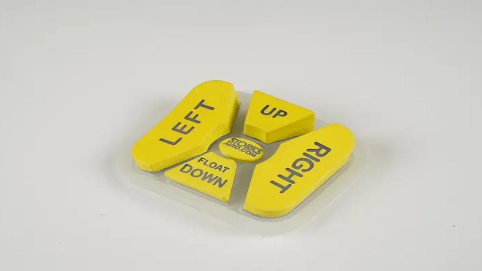
A silicone rubber keypad is a molded elastomer interface that guides a finger press, stores and releases mechanical energy in a web or dome, and transfers motion to an electrical contact system. The molded part may carry a conductive pill, press a metal dome, actuate a separate switch, or serve only as a sealed mechanical keymat. Shin-Etsu Polymer describes the familiar rubber-contact form as a silicone dome whose geometry and material create a force–travel response; its contact element closes against the circuit beneath it. Shin-Etsu's force–travel definitions provide the terminology used in this guide.
A keypad is not automatically a complete switch assembly. It is also not a touchscreen, a finished enclosure, or evidence of an ingress rating. The electrical event depends on the circuit, contact pattern, closing load, support, housing, and firmware threshold. The environmental result depends on the assembled enclosure and its tested interfaces.
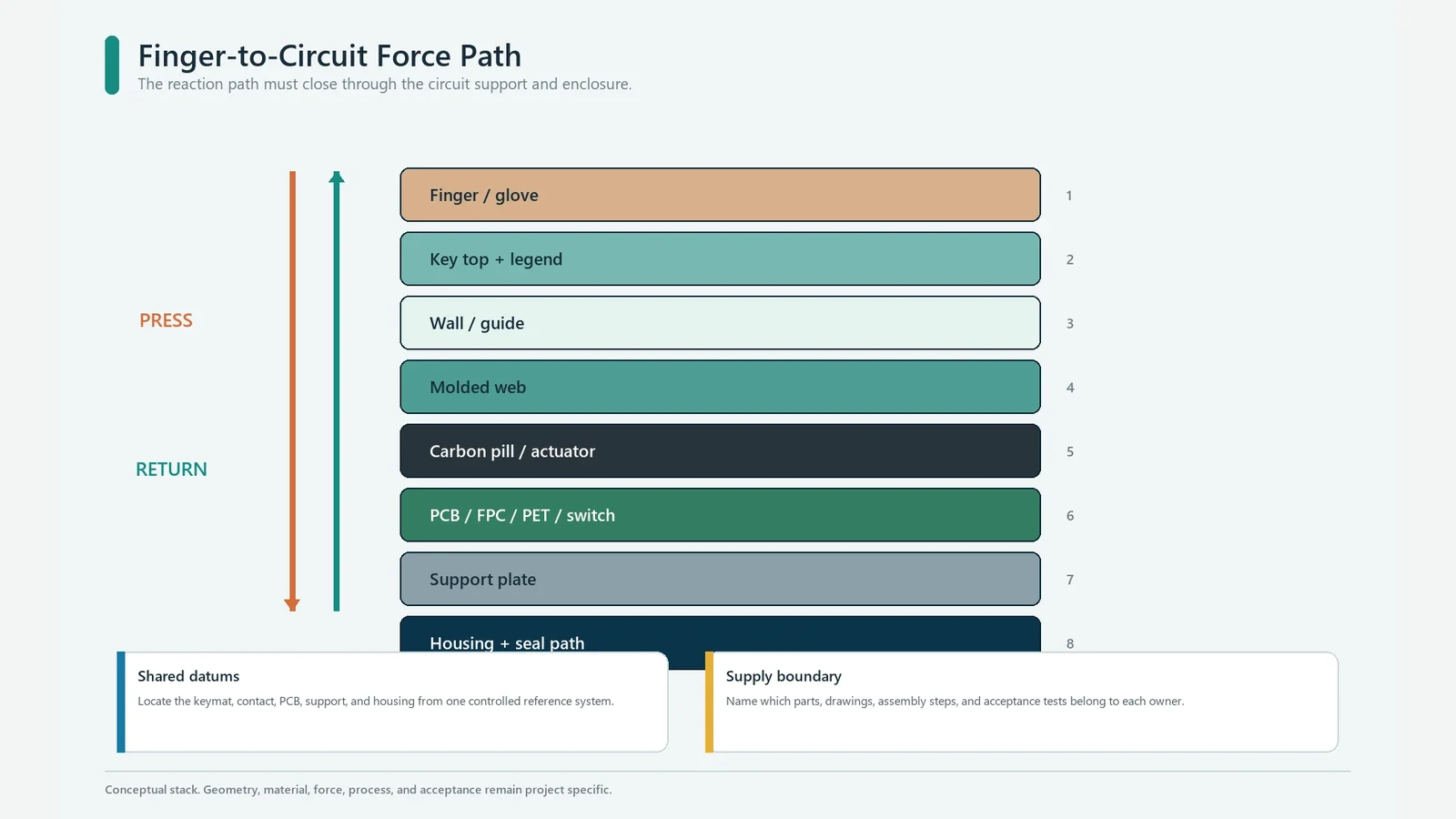
Canonical finger-to-circuit stack:
Finger → keytop and legend → guide or bezel → molded web → plunger/contact carrier → conductive element or separate switch → PCB, FPC, or PET circuit → rigid support → housing, fasteners, and seal path
Each arrow is an interface. Each interface needs an owner.
| Stack element | Function to control | Required project input | Failure if left implicit |
|---|---|---|---|
| Keytop and legend | Locates the finger and communicates the command | Top shape, size, artwork, color, texture, viewing condition | Mis-presses, poor readability, artwork outside the printable zone |
| Guide or bezel | Limits lateral motion and protects edges | Clearance, datum, side-load condition, cosmetic gap | Rubbing, wobble, keys that do not return |
| Molded web | Produces the spring response | Section geometry, radii, material family, press/release targets | Wrong peak force, weak return, tearing, key-to-key variation |
| Plunger or carrier | Transfers motion toward the circuit | Centerline, height, hard-stop relationship, angular tolerance | Off-center loading or excessive circuit load |
| Contact element | Creates or transfers the electrical event | Type, size, retention, location, closing load, test fixture | Intermittent closure, unstable resistance, contamination sensitivity |
| PCB, FPC, or PET circuit | Receives the contact | Pad geometry, finish, spacing, support, electrical threshold | Contact mismatch, flex, shorting, bounce, false acceptance |
| Support structure | Controls deflection and bottoming | Material, thickness, flatness, fastening, local support | A good loose key becomes a poor installed key |
| Housing and seal path | Sets compression, venting, alignment, and ingress boundary | Datums, closure load, gasket path, vent route, full test configuration | Preload drift, trapped air, leaks, distorted feel |
The design boundary should be named before CAD begins: loose molded keymat, keymat plus circuit, tested module, or complete enclosure. A force curve approved on a rigid bench plate does not automatically approve the same key over a flexible PCB. Likewise, IEC 60529 classifies protection provided by an electrical enclosure. A molded perimeter bead or loose keypad alone does not establish IP65, IP67, or IP68.
Design rule: control the complete installed stack, not the silicone silhouette by itself.
2. How a Silicone Key Converts Force into an Electrical Event
A silicone key does not switch at one isolated force number. It follows a path. The web first resists motion, reaches a peak, drops toward the contact point, closes the circuit, travels far enough to maintain stable contact, and then returns along a different curve when the finger lifts. A useful specification records both press and release traces.
The physical sequence is straightforward:
- The finger loads the keytop while the guide, bezel, and housing constrain lateral motion.
- The molded web deforms and stores elastic energy. Web section, radii, key height, compound, cure state, and side load all influence the curve.
- The plunger or molded carrier brings the contact element toward the circuit.
- The electrical state changes when the contact bridges the specified PCB, FPC, or PET pattern under a defined closing load.
- The hard stop, circuit support, and available overtravel limit further motion. On release, the web must lift the contact clear and return the key without binding.
Shin-Etsu Polymer uses F1, F2, S1, and S2 to describe the characteristic curve. The same public page defines click ratio as (F1 − F2) / F1 × 100%. The source diagram and equation are useful because they name both force and travel; the equation does not create a universal target.
| Curve event | Drawing definition | Why it matters | Common mistake |
|---|---|---|---|
| Rest and preload | Installed zero, any housing compression, probe contact, and circuit support state | Preload can shift the entire press and release record | Zeroing a loose part, then accepting an installed assembly |
| F1: peak force | Maximum force before the principal force drop on the press trace | Captures the initial effort and web transition | Writing only “actuation force” without defining the event |
| S1: peak travel | Travel coordinate at F1 | Connects the force peak to geometry | Reporting F1 and travel from different traces |
| F2: make/contact force | Force at the defined mechanical or electrical contact event | Shows the force maintained when the circuit closes | Confusing contact force with contact resistance |
| S2: contact travel | Travel coordinate at the defined contact event | Sets the stack height and circuit relationship | Measuring contact on a different PCB pattern |
| Stable-contact zone | Allowed travel and load after first closure | Provides contact margin before bottoming | Treating first continuity as a complete approval |
| Mechanical end stop | Housing, key, or support feature that limits load | Protects the circuit and stabilizes bottom feel | Letting the PCB become the uncontrolled hard stop |
| Release and return | Release point, minimum return behavior, residual preload, and hysteresis | Confirms separation and key recovery | Approving the press trace but never recording release |
Variable names beyond F1, F2, S1, and S2 are not consistent across supplier literature. For example, an F3 label may refer to an end-stop load in one diagram and a return-related force in another. A controlled specification should define the event beside every symbol rather than rely on the symbol alone.
Snap ratio, key ratio, and web ratio are not interchangeable
If key ratio means the tactile snap ratio, write the F1/F2 equation and the event definitions. If it means a geometric proportion, state the two dimensions, section, datums, and measurement direction. If it means web ratio, replace that bare phrase with a controlled geometry definition.
No reviewed ASTM, IEC, ISO, WACKER, or Shin-Etsu material source establishes one universal silicone-keypad web-ratio formula. Web geometry is a field of thicknesses, angles, radii, tapers, anchors, and local transitions. Reducing it to one undocumented number hides the feature that the toolmaker must actually cut.
The planned companion article on silicone keypad force, travel, and web ratio will own the detailed measurement method.
Engineering reference baseline for initial samples
No industry standard mandates a default keypad feel. The following source-backed values form one coherent initial sample baseline. Final values must match the approved material, geometry, assembly, and test method.
| Parameter | Initial reference value | Source condition | Project release input |
|---|---|---|---|
| Material hardness | 55 ± 5 Shore A | N&H typical keypad baseline | Verified compound, scale, method, location, and tolerance |
| Peak actuation force F1 | 180 ± 50 cN, equivalent to 1.8 ± 0.5 N | N&H typical keypad baseline | Project force target, key group, installed test state, and tolerance |
| Snap ratio | 50 ± 10% | N&H supplier baseline using its defined force events | Approved F1/F2 equation, return requirement, and project tolerance |
| Key stroke | 1.1 ± 0.1 mm | N&H typical keypad baseline | Project S1/S2 and end-stop travel definitions with tolerances |
| Initial web-thickness discussion point | About 0.5 mm | MekoPrint supplier rule-of-thumb, dependent on hardness and layout | Molder-reviewed section geometry and sampled force–travel result |
Sources: N&H silicone rubber keypad design guide and MekoPrint HMI design guide. Keep the original cN and mm context in the controlled record.
Shore hardness is not key feel
ASTM D2240 measures indentation hardness with named durometer types under specified conditions. ASTM describes it as an empirical control test influenced by indenter geometry, applied force, elastic modulus, and viscoelastic behavior. It does not measure the force–travel curve of an assembled key.
Two keypads molded from compounds with the same nominal Shore A result can feel different when the web, key height, contact location, preload, support, cure state, or housing clearance changes. The drawing should therefore name the hardness scale and test method, then specify the installed force–travel behavior separately.
Compression set is another separate property. ASTM D395-18(2025) addresses recovery after defined static compressive exposure and distinguishes constant-force from constant-deflection methods. It matters where a seal or keypad remains compressed, but it does not replace repeated flexing, return, or key-cycle validation.
The planned silicone keypad hardness and compression-set selection article will carry the deeper material-selection method.
The contact interface deserves the same discipline. A conductive rubber keypad may use a molded carbon contact, conductive print, a plated element, or another architecture. Shin-Etsu's published contact table ties its values to a named PCB pattern and test setup, demonstrating why resistance cannot be separated from pad geometry, finish, closure load, and method. Contact-element reference.
Measurement rule: approve a named press event, release event, electrical event, test state, and fixture—not a free-floating force or ratio.
3. Silicone Rubber Keypad Design Guide: 10 Decisions Before Tooling
The safest rubber keypad design rules are decision rules, not copied dimensions. Ten decisions control most of the risk: product boundary, material, force–travel behavior, key role, web geometry, contact system, surface graphics, lighting, enclosure integration, and production approval. None should remain as a toolmaker assumption.
| # | Decision | Controlled output | Acceptance evidence | Stop condition |
|---|---|---|---|---|
| 1 | Product and supply boundary | Loose keymat, keypad plus circuit, tested module, or complete enclosure | One owner for every finger-to-circuit interface | RFQ and drawing describe different supplied assemblies |
| 2 | Material system | Material family, named grade or approval process, hardness method, color, cure/post-cure requirements | Grade-linked data and a controlled change route | “Silicone, 50 hardness” with no scale, method, or grade policy |
| 3 | Force–travel response | Press and release curves, F1/F2/S1/S2, return, overtravel, hard stop, test state | Events and tolerances defined on the installed stack | One force target copied across unlike keys |
| 4 | Key roles and geometry | Keytop, guide, web sections, radii, height, spacing, centerline, side-load case | Functional dimensions tied to datums | Cosmetic CAD with no web section or contact center |
| 5 | Contact and circuit | Contact type, retention, PCB pattern/finish, closing load, support, electrical threshold | One matched contact-plus-circuit test fixture | Carbon-pill value quoted without the PCB and load |
| 6 | Legends and surface | Artwork, print zone, color reference, texture, coating stack, wear/cleaner method | Approved visual master and objective damage limit | “Permanent printing” with no exposure or acceptance rule |
| 7 | Backlighting | LED type/location/current, transmissive stack, mask, brightness/uniformity zones, ambient states | Powered sample in the real housing | Legend approved unpowered or outside the enclosure |
| 8 | Enclosure and sealing | Seal path, compression, vent route, fasteners, housing datums, ingress test configuration | Complete-enclosure drawing and test plan | IP rating assigned to a loose molded part |
| 9 | Molding and tooling | HCR/LSR route, parting line, gates, vents, flash zones, shrink study, cavity ID, correction plan | Process route chosen before steel release | Tool released while the compound or sealing surface is undefined |
| 10 | Assembly and validation | Support, preload, connectors, firmware threshold, sample matrix, change control, release evidence | Golden data set tied to revision and cavity | Cosmetic sample treated as production approval |
3.1 Separate key roles before tuning feel
Not every key deserves the same curve. A power key, emergency function, repeated navigation key, numeric entry key, and hidden service key have different accidental-activation and repetition risks. Group keys by function, operator, glove condition, posture, and expected use. Then define a curve family for each group.
This step prevents a common failure: one nominal force is copied across keys with different widths, heights, legends, guides, and contact locations. Even if the peak force matches, return, wobble, contact timing, and bottom feel may not. Approve representative corner keys, long keys, small keys, and high-use keys—not only the easiest central key.
3.2 Geometry makes the spring
The web is a molded spring, but its behavior does not come from thickness alone. Inner and outer anchors, section transitions, angles, radii, local taper, key height, keytop moment arm, guide clearance, compound, and cure state all contribute. Side load can change the response again.
Control these geometric relationships:
- The finger load should enter the intended keytop area without creating excessive moment.
- The key guide should prevent harmful lateral motion without rubbing during the full press and release path.
- The web should transition through smooth, manufacturable sections rather than an unreviewed sharp corner.
- The plunger or contact center should land on the circuit datum under worst-case registration.
- A deliberate hard stop should limit load before the PCB, coating, or contact element becomes the stop by accident.
- Vent paths should let displaced air move without opening a sealed perimeter to the outside environment.
Supplier guides publish different web and clearance starting points because their materials, tools, geometries, and test methods differ. That conflict is useful evidence against a universal rule. The molder should return a sectioned DFM proposal and a predicted or sampled force–travel response; the OEM should approve the installed result.
3.3 Treat the contact and PCB as one matched interface
Carbon pills are common, but they are not the only option. Shin-Etsu Polymer lists carbon-silicone print, molded carbon elements, lower-resistance carbon variants, plated contacts, and metal-dome constructions as distinct choices. Each changes resistance behavior, thickness, retention, force path, cost structure, and test method. Shin-Etsu contact-element overview.
The release package should define the contact element and the mating circuit together. At minimum, name the contact size and location, retention method, PCB pad pattern, conductor finish, pad spacing, circuit support, electrical threshold, applied closing load, conditioning, and measurement fixture. A carbon-pill sample approved on a gold reference coupon is not automatically approved on the production PCB.
Detailed resistance and fixture comparisons belong to the planned conductive carbon pill resistance resource rather than a universal number in this design guide.
First closure is not the only event. Confirm stable closure through allowed overtravel, separation on release, contact behavior under off-center press, and the effect of housing preload. If firmware debounce or threshold logic affects the accepted event, version it with the hardware evidence.
3.4 Design artwork, coating, and backlighting as a stack
Printed legends, molded colors, coated surfaces, laser-opened legends, and hard keycaps solve different problems. The choice should begin with viewing distance, ambient light, glove use, cleaner exposure, abrasion mechanism, tactile locator needs, color tolerance, and service environment.
For a backlit laser-opened key, Shin-Etsu describes a construction that starts with molded silicone, adds a transmissive image-color layer and dark masking layer, removes the symbol by laser, then applies a protective overcoat. HG keypad construction. That stack is one documented architecture, not a life claim or a JASPER process claim.
Light uniformity depends on more than the LED. MekoPrint's 2025 design guide identifies silicone thickness, pigment, LED location, masking, and housing geometry as coupled optical inputs. A backlit silicone rubber keypad should therefore be approved as a powered stack at defined current, ambient state, viewing angle, and housing build.
For laser-etched silicone keypads, freeze artwork only after the printable or laserable zone is known. Specify acceptable edge quality, light leak, color, gloss, icon registration, and wear. IEC 60068-2-70 can support a finger/hand abrasion method, but the product specification still has to select severity, fluid, conditioning, and failure criteria.
The planned laser-etched legend and protective-coating guide will own the detailed coating, laser, cleaner, and abrasion choices.
3.5 Sealing belongs to the enclosure
A molded keypad can form part of a seal, yet the tested boundary includes housing surfaces, fasteners, compression, adhesive or gasket, cable exits, circuit openings, vents, and assembly variation. The seal path should be drawn in section and tied to common datums. Closure load and compression should be controlled without preloading the key webs into a different force state.
Trapped air is a separate design problem. Internal vent channels may connect key cavities while preserving the outer seal boundary; their geometry and route require molder review. An external opening may relieve pressure but can defeat the intended enclosure boundary. The correct choice follows the complete housing and test configuration, not a generic keypad sketch.
An ingress code is accepted only after the complete configuration is tested to the invoked requirement. IEC 60529 edition 2.2 applies to protection provided by enclosures; automotive programs may invoke a different standard or OEM method. The drawing and report should identify the tested revision, orientation, fastener condition, cable state, preconditioning, and post-test functional checks.
every design decision needs a controlled output, an evidence owner, and a tool-release stop condition.
4. Choose Material, Molding Route, and Tool Strategy Together
Material selection is a system decision. WACKER distinguishes solid high-consistency rubber from two-component liquid silicone rubber and documents compression, transfer, and injection routes. Process choice depends on the required cured properties, material family, part geometry, series size, equipment, and available expertise. WACKER's material and processing guide is the primary source for this boundary.
Neither HCR nor LSR is universally better for a keypad. The right route is the one that can produce the required webs, contacts, colors, surfaces, inserts, cavity count, and inspection evidence with an agreed correction plan.
| Material/process path | Source-backed characteristic | Design consequence | Questions before release |
|---|---|---|---|
| HCR with compression molding | Solid compound is placed into the mold as a controlled charge; WACKER treats compression as a distinct press-molding route | Charge placement, flow, flash, color placement, inserts, and cavity balance need review | Which grade and cure system? How are charges controlled? Where are parting lines and flash allowed? |
| HCR with transfer or injection molding | Solid silicone can also be processed through transfer or injection routes | Runner, gate, flow, vent, and insert strategy differ from simple compression assumptions | Why is this route selected? What geometry or automation benefit does it provide? |
| LSR with injection molding | LSR is a lower-viscosity, two-component addition-cure family in the cited WACKER portfolio | Low viscosity changes gate, vent, flash-control, and handling decisions; tool design must match the selected grade | What are the material data, mixing controls, gate/vent locations, flash limits, and demolding plan? |
| Secondary finishing | Post-cure, deflashing, bonding, coating, printing, and laser operations occur after molding when required | A dimension or color approved before finishing may shift or look different afterward | Which operations occur, in what order, and which state owns final inspection? |
Shrinkage shows why the compound cannot remain a late purchase choice. The WACKER reference gives an approximate 2–4% linear range across its broad silicone discussion. Actual shrinkage depends strongly on material grade and process. That number is not a recommended keypad allowance. The controlled tool factor must come from the selected compound data, tool-temperature assumptions, geometry, and molder trials.
The same caution applies to post-cure. WACKER explains that post-curing can alter properties such as compression set and remove volatile components, but schedule and need depend on grade, section, and application. The OEM drawing should state the required finished state and evidence. It should not paste a handbook temperature/time example into a part specification.
Tool release needs a surface-by-surface review
Tooling questions should be answered on the 3D model and a marked 2D drawing:
- Which surfaces form the key web, seal, guide, artwork zone, and circuit datum?
- Where are the parting line, gates, vents, overflows, eject or handling features, and expected vestiges?
- Which flash zones are functional, cosmetic, seal-critical, or hidden?
- Which radii, undercuts, initial directions, and shutoffs are tooling-controlled?
- How are contact inserts retained and centered?
- Which dimensions are tool-bound, closure-dependent, finishing-dependent, or measured only after conditioning?
- How are cavities identified, sampled, corrected, and compared after a change?
Low-viscosity LSR can enter very small mold gaps. Review parting lines, gates, vents, overflows, and flash-sensitive surfaces deliberately. Its guidance also advises keeping parting lines off sealing surfaces where practical. LSR design considerations. These are tool-interface questions, not JASPER capability claims or global tolerances.
ISO 3302-1:2014 defines dimensional-tolerance classes for molded solid rubber products and the related compliance basis. A drawing may invoke an agreed class, but force-critical webs, contact registration, and assembly datums still need specific control. Passing a general rubber tolerance class does not prove the force curve.
The cluster's planned silicone keypad tooling and prototyping article can carry cavity correction, sample stages, and tool-approval detail while this guide keeps the system-level release boundary.
JASPER's actual material grades, HCR/LSR scope, molding routes, post-cure practice, tool source, cavity-correction method, and in-house versus external operations are project confirmation required in the sources reviewed for this article. They must be confirmed for the project before any JASPER-specific statement or tool commitment.
Tooling rule: freeze compound, process route, finished state, tool interfaces, shrink strategy, and correction ownership together.
5. How to Build a Silicone Keypad Drawing Package
A useful silicone keypad drawing package is more than a 3D shape. The 3D model defines surfaces; the 2D drawing defines controlled requirements, datums, states, and acceptance. Circuit, artwork, optical, environmental, and assembly files close the interfaces that neither CAD file can carry alone.
| Package item | Minimum controlled content | Approval owner |
|---|---|---|
| 3D CAD model | Nominal finished geometry, keytops, webs, guides, plungers, seals, vents, undercuts, assembly context | Mechanical engineering |
| 2D part drawing | Revision, units, datums, functional dimensions, agreed tolerance basis, hardness method, color, surface zones, notes | Mechanical and quality engineering |
| Force–travel specification | Test state, probe, direction, speed, preload, support, F1/F2/S1/S2 definitions, return, overtravel, hard stop, tolerances | Human factors and mechanical engineering |
| Circuit package | PCB/FPC/PET revision, pad pattern, finish, stack thickness, support, connector, electrical threshold, firmware dependency | Electrical engineering |
| Contact definition | Type, material/product reference, size, location, retention, closing load, resistance method, fixture | Electrical and supplier engineering |
| Artwork master | Vector artwork, font handling, positive/negative legend intent, color references, registration datums, protected zones | Industrial design and brand owner |
| Optical specification | LED part, location, drive state, transmissive and masking layers, brightness/uniformity zones, ambient and viewing states | Optical and electrical engineering |
| Enclosure section | Bezel clearance, seal path, compression, fasteners, support, venting, cable exits, full ingress-test configuration | Mechanical engineering |
| Validation matrix | Sample stages, quantities by cavity/position, conditioning, methods, limits, failure definitions, report format | Quality and design assurance |
| Supply-boundary record | Loose keymat or module, included circuit/LED/connector/housing, packaging, change control, traceability | Sourcing, supplier quality, and operations |
Functional dimensions deserve explicit treatment. A key center may be dimensionally acceptable relative to the rubber edge yet miss the PCB contact when the housing locates both parts from different datums. The drawing should show the relationship that matters: key center to circuit center, seal bead to housing land, guide to bezel, plunger to hard stop, and contact to supported pad.
Conditioning and timing also affect comparisons. ISO 23529:2016 covers preparation, storage, conditioning, and the interval between forming and testing rubber test pieces. It does not define a whole-keypad test, but it supports a crucial rule: sample age, conditioning, and test environment belong in the record when two curves or lots are compared.
Use six approval gates
The approval flow should convert risk into evidence in small steps. JASPER's public prototyping and sample approval page describes prototype planning as a sequence of decisions rather than one cosmetic sample. The project-specific gates below make that sequence concrete.
| Gate | Evidence required | Release decision |
|---|---|---|
| 1. Requirements freeze | Operator, environment, key roles, architecture, supply boundary, target circuit, risk list | Is molded silicone the right interface, and is the project boundary complete? |
| 2. DFM and stack review | Sectioned 3D model, marked 2D drawing, material/process proposal, tool-interface markup, force-curve plan | Are all critical interfaces manufacturable and owned? |
| 3. Tool-design review | Parting line, gates, vents, flash zones, cavity ID, shrink strategy, inserts, correction access | Can steel be released without guessing a seal, web, contact, or cosmetic surface? |
| 4. Mechanical sample | Dimensions, fit, preload, wobble, force–travel press/release traces, return, hard stop, contact alignment | Does the installed mechanical stack meet the controlled intent? |
| 5. Decorated powered assembly | Production-intent contact/circuit, legends, coating, LEDs, housing, firmware state, visual master | Do electrical, optical, surface, and assembly interfaces pass together? |
| 6. Production release | Cavity/position evidence, validation matrix, approved data set, inspection plan, packaging, change record | Is the production state reproducible and traceable? |
Do not merge these gates into “sample approved.” A color sample cannot approve web life. A loose force coupon cannot approve enclosure preload. A working electrical sample cannot approve legend wear or seal integrity. Each sample needs a written decision purpose and a revision.
The silicone keypad sample approval checklist provides the detailed release checklist.
The supplied-assembly boundary matters throughout. A silicone keypad assembly can include more interfaces than a loose molded part, so the release package should state which party owns PCB support, LEDs, connector, housing fit, programming, final functional test, and packaging. The linked page shows a public product route; actual project scope remains subject to written confirmation.
Drawing rule: the package is complete only when a reviewer can reconstruct geometry, force, circuit, optics, enclosure, test state, and supply boundary without asking the toolmaker to choose them.
6. Validate the Installed System, Not a Loose Keymat
Validation should reproduce the operating state users will press. That normally means production-intent housing, circuit support, contact pattern, fasteners, preload, LEDs, connector, and firmware. Loose-part tests still have value for process control, but their acceptance boundary must be named.
There is no universal keypad test package. JASPER's public testing and validation planning page makes the same boundary explicit: requirements, samples, production evidence, and changes create separate gates. The matrix below converts that principle into project inputs.
| Characteristic | Test state and method fields | Acceptance evidence | Standard boundary |
|---|---|---|---|
| Dimensions and registration | Conditioned finished part; datum scheme; measurement equipment; cavity and position | Report tied to part revision and cavity | ISO 3302-1 may provide a class; critical interfaces still need specific controls |
| Material hardness | Named specimen or part location; durometer type; conditioning; dwell; method edition | Result linked to compound/lot and scale | ASTM D2240 does not approve key feel |
| Press/release force–travel | Installed support and housing; probe; direction; speed; preload; cycles before reading; force in N; travel in mm | Full traces with extracted F1/F2/S1/S2, return, and hard-stop events | Project method; no cited standard supplies a universal keypad curve |
| Electrical closure | Production-intent contact, PCB pattern/finish, support, closing load, threshold, data acquisition | Closure, stable-contact, release, and repeat records | Supplier resistance tables are comparable only when fixtures match |
| Legend and coating | Production finish; finger abrasion or project wear medium; cleaners; conditioning; visual/dimensional damage limit | Before/after images and objective pass rule | IEC 60068-2-70 can support marking abrasion, with project-selected severity |
| Backlight | Production LEDs, current, mask, coating, housing, ambient states, viewing angles | Brightness/uniformity map and approved visual master | No generic LED spacing or brightness target |
| Enclosure ingress | Complete enclosure, cable state, fasteners, orientation, preconditioning, post-test function | Scoped report for the exact assembly revision | IEC 60529 applies to enclosure protection, not the loose keypad |
| Environmental exposure | Named temperature, humidity, fluids, dwell, transitions, powered/unpowered state | Functional and material checks before, during, or after exposure as specified | Conditions come from the product environment and invoked requirement |
| ESD immunity | Complete powered equipment, discharge points, grounding, operating modes, performance criteria | Equipment-level report and recovery behavior | IEC 61000-4-2:2025 is not a bare-silicone material claim |
| Key cycling | Installed load path, travel or overtravel, frequency, environment, circuit, sample/cavity plan, failure definition | Curve, electrical, visual, and crack evidence at defined intervals | A cycle count without conditions is not transferable |
Diagnose failures from evidence
A failed key is a symptom, not a root cause. Preserve the curve, assembly state, sample identity, cavity, circuit, and environmental history before changing the web or compound.
| Symptom | Possible interface chain | Evidence to inspect first | Controlled next action |
|---|---|---|---|
| Peak force is high only after assembly | Housing compression → web preload → shifted F1/S1 | Loose and installed curves; closure height; fastener sequence | Correct stack or preload before changing material hardness |
| Key closes but returns slowly | Guide rub, side load, trapped air, low return margin, surface contamination | Release trace; side-load video; vent path; witness marks | Isolate guide, vent, and return contributors one at a time |
| Contact is intermittent | Pill registration → PCB pattern/finish → support flex → closing load → contamination | Contact map; production PCB; support deflection; synchronized force/electrical trace | Fix the matched contact/circuit interface, not just the pill |
| One key or cavity drifts | Local tool section, vent, flash, insert placement, cure, or measurement alignment | Cavity/position data; section measurements; process record | Compare like positions and correct the identified source |
| Legend or coating wears early | Surface preparation → ink/coating stack → cure → cleaner/abrasion exposure | Batch trace; cross-section; adhesion and wear record | Requalify the complete finish stack under the actual exposure |
| Backlight shows hotspots or leaks | LED location → pigment/thickness → mask → coating → housing reflection | Powered optical map; layer samples; housing build | Tune the optical stack and reapprove the powered assembly |
| Enclosure leaks | Seal land → compression → parting/flash → fastener/cable state → vent route | Leak location; section compression; assembly record | Repair the complete seal path and retest the exact configuration |
A golden sample can aid visual comparison, but it should not replace numeric data, drawings, or approved traces. Store the sample revision, material lot, cavity, conditioning, and measurement record. If the compound, tool, contact, PCB finish, coating, LED, housing, or test method changes, reopen the affected evidence instead of carrying approval forward by assumption.
Validation rule: validate the production-intent stack, preserve failure evidence, and tie every pass to a revision, method, condition, and sample identity.
7. Where Silicone Keypads Fit—and When They Do Not
Silicone keypad design works best when a product needs molded key geometry, a tunable force path, tactile location, color or lighting options, and an elastomer interface that can participate in the enclosure. The application name alone does not select the construction.
| Use case | Silicone is a candidate when | Inputs that control the decision | Boundary to preserve |
|---|---|---|---|
| Industrial controls | Operators need raised, locatable keys, possibly with gloves or limited sight | Glove type, target size/spacing, side load, contaminants, cleaning, viewing and lighting | Validate the complete panel, support, legends, and enclosure |
| Medical or laboratory equipment | A molded interface supports the required human factors and cleaning workflow | Contact type/duration, cleaner list, use environment, risk controls, device-level requirements | Component material data do not establish finished-device validation or regulatory approval |
| Automotive controls | Key feel, packaging, lighting, and appearance must work in a defined mounting location | Temperature profile, vibration, sunlight, chemicals, gloves, illumination, vehicle test plan | Use the invoked OEM and assembly requirements; do not transfer a generic keypad limit |
| Marine or outdoor equipment | Raised keys and an integrated seal concept suit the housing | Salt, water, UV, temperature cycling, cable exits, venting, fasteners, housing stiffness | Test the complete enclosure; the keypad alone does not own the ingress code |
| Handheld and portable devices | One molded part can combine multiple keys, tactile cues, color, and a contact carrier | Drop loads, pocket activation, battery/PCB support, thin-stack target, cosmetic wear | Compare total stack height, tooling commitment, and field-service needs with alternatives |
Molded silicone is not the best choice in several common situations:
- A very thin, flat interface with printed graphics and little key height may favor a membrane keypad.
- A frequently changing interface, large dynamic display, or gesture input may favor capacitive touch plus a deliberate haptic strategy.
- A function that needs a standard discrete switch with a tightly characterized off-the-shelf mechanism may not benefit from a custom molded web.
- Continuous rotation, proportional analog control, or a guarded emergency mechanism may require a different control architecture.
- A low-volume program with unsettled geometry may not justify production tooling until the architecture and demand are stable.
The decision should compare the full system: stack height, user feedback, sealing, graphics, lighting, circuit, assembly, test burden, tool changes, and service strategy. The live membrane keypad versus silicone keypad comparison provides a related architecture check without changing this article's design-guide intent.
JASPER also publishes a silicone keypad control interface case as related reading. A case page can show how interfaces are framed, but it does not prove that another program should use the same material, contact, geometry, test, or result.
Architecture rule: choose molded silicone only after the operator, complete stack, environment, validation burden, and alternative architectures have been compared.
8. Frequently Asked Questions
What Shore hardness should an OEM specify for a silicone keypad?
No Shore A value guarantees the required key feel. This guide uses 55 ± 5 Shore A only as a clearly labeled initial baseline from one established supplier guide. Replace it with the approved compound, ASTM D2240 or other named method, specimen/location, tolerance, and installed force–travel targets before release and tool release.
What is the correct web ratio for a silicone rubber keypad?
No reviewed authority defines one universal keypad web ratio. If the term means snap ratio, state (F1 − F2) / F1 × 100%. If it means geometry, define the numerator, denominator, section, datums, measurement direction, and finished condition. A bare ratio should never control the mold.
How should force and travel be specified?
Specify full press and release traces in a named test state. Define the probe, direction, speed, preload, support, conditioning, F1, F2, S1, S2, stable-contact zone, return event, overtravel, and hard stop. Record force in N and travel in mm while preserving any approved source units.
Can a carbon pill be approved without the final PCB?
A reference coupon can screen the contact, but it cannot approve the production interface. Final acceptance needs the intended contact, PCB pad pattern and finish, circuit support, closing load, electrical threshold, conditioning, and measurement method. Contact-resistance figures from different fixtures should not be compared as equivalent.
What belongs in a silicone keypad drawing package?
Include a revision-controlled 3D model, 2D drawing, force–travel specification, production-intent circuit, contact definition, vector artwork, optical requirements, enclosure sections, validation matrix, and supply-boundary record. The package should identify functional datums, critical states, test conditions, approval owners, and change-control rules.
Can the molded silicone keypad itself have an IP rating?
No loose keypad establishes the finished enclosure's IP rating. IEC 60529 classifies protection provided by the tested electrical enclosure. The report must identify the housing, keypad, seal, fasteners, cable state, orientation, preconditioning, and post-test function for the exact assembly revision.
How should backlit or laser-etched legends be approved?
Approve the production-intent powered stack: silicone, pigment, transmissive layer, dark mask, laser opening or print, protective coating, LED, drive current, housing, ambient light, and viewing angle. Define uniformity, hotspot, light-leak, color, registration, abrasion, cleaner, and visible-damage criteria.
When is silicone keypad tooling ready for release?
Release tooling only after the material/process route, web sections, contact and PCB, force–travel method, hard stop, seal path, vents, parting line, gates, flash zones, artwork, optical stack, assembly datums, sample stages, correction ownership, and acceptance matrix are controlled under the same revision.
9. Send a Keypad Drawing or 3D Model
The next useful action is a controlled design review. Send a keypad drawing or 3D model with the mating circuit, enclosure section, key-role list, initial force–travel targets, contact choice, artwork, lighting stack, environment, validation matrix, and required supply boundary.
Mark unknowns as unknowns. A supplier can propose a compound, web, tooling route, contact, or coating, but the proposal should return as a revision-controlled DFM record with assumptions and evidence—not disappear into tool steel.
Project review must confirm the offered material, molding route, tool boundary, secondary operations, test method, assembly scope, evidence, MOQ, and lead time in writing.
Before purchase order or tool release, confirm every initial value in the controlled drawing and approval record.
Technical References
- Source: WACKER Solid and Liquid Silicone Rubber Material and Processing Guidelines. Accessed 2026.
- Source: Shin-Etsu Chemical Characteristic Properties of Silicone Rubber Compounds. Accessed 2026.
- Source: Shin-Etsu Polymer Force-Travel Characteristic. Accessed 2026.
- Source: Shin-Etsu Polymer Contact Elements for Keypads. Accessed 2026.
- Source: N&H Technology Design Guide for Silicone Rubber Keypads. Accessed 2026.
- Source: MekoPrint HMI Design Guide for Silicone Rubber Keypads. Accessed 2026.
- Source: ASTM D2240-15(2021) Durometer Hardness. Accessed 2026.
- Source: ASTM D395-18(2025) Compression Set. Accessed 2026.
- Source: ISO 3302-1:2014 Rubber Product Dimensional Tolerances. Accessed 2026.
- Source: ISO 23529:2016 Rubber Test-Piece Conditioning. Accessed 2026.
- Source: Shin-Etsu's force–travel definitions. Accessed 2026.
- Source: IEC 60529. Accessed 2026.
- Source: The source diagram and equation. Accessed 2026.
- Source: N&H silicone rubber keypad design guide. Accessed 2026.
- Source: MekoPrint HMI design guide. Accessed 2026.
- Source: ASTM D2240. Accessed 2026.
- Source: ASTM D395-18(2025). Accessed 2026.
- Source: Contact-element reference. Accessed 2026.
- Source: Shin-Etsu contact-element overview. Accessed 2026.
- Source: HG keypad construction. Accessed 2026.
- Source: IEC 60068-2-70. Accessed 2026.
- Source: WACKER's material and processing guide. Accessed 2026.
- Source: LSR design considerations. Accessed 2026.
- Source: ISO 3302-1:2014. Accessed 2026.
Review the keypad construction before tooling release
Send the drawing, key geometry, force targets, contact stack, artwork, housing, environment, and approval plan for a construction-specific review.