
Electrode-site map
Release controlRelease every site, size, shape, coordinate, channel or function name, reference feature, orientation, and datum.
If it is missingManufacturing receives an image without controlled geometry or site identity.
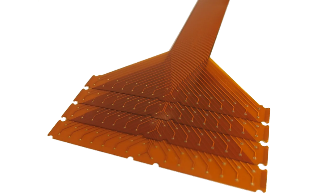
Custom printed electrode arrays are the broad route for OEM and research projects whose site map does not fit a standard patch label. JASPER can manufacture application-specific electrode sites, conductive traces, dielectric or insulation zones, flexible substrates, tails, connector lands, reinforcement, project-defined converted layers, die cutting, labels, packaging, and agreed inspection. The customer owns the electrical function, use conditions, system behavior, safety, clinical or research conclusions, and regulatory validation.
A custom array may support sensing, stimulation research, contact measurement, human-machine interaction, laboratory instrumentation, or another OEM-defined purpose. The route name does not assign a medical claim; the released circuit and responsibility matrix define the supply.
JASPER can review printability, layer registration, flexible interconnect, converting, and inspection. The customer must define functional electrical limits, mating electronics, installation, use conditions, data or actuation interpretation, safety, and any clinical or regulatory pathway.
Start with the electrical artwork, then close the material and mechanical conversion around it.
Release every site, size, shape, coordinate, channel or function name, reference feature, orientation, and datum.
If it is missingManufacturing receives an image without controlled geometry or site identity.
Define ink, widths, clearances, routing, crossovers, guards, insulation openings, flex zones, continuity, resistance, and isolation.
If it is missingThe circuit is printable but does not meet the customer interface or electrical acceptance.
Release conductor pitch, tail outline, bend zones, reinforcement, connector lands, connector, pin map, and mating part.
If it is missingThe array cannot connect or flex in the intended installation.
Name substrate, backing, adhesive or hydrogel zones, foam or nonwoven, liner, labels, reinforcement, and material boundaries.
If it is missingLayer overlap changes active openings, stiffness, edge exposure, or assembly access.
Control circuit datum, outside profile, holes, slots, openings, layer overlap, tail exit, tolerance, and inspection fixture.
If it is missingThe printed sites and mechanical features do not align in the finished array.
Define dimensions, electrical method, interface checks, visual criteria, label, package, lot records, substitutions, and requalification.
If it is missingA changed material or geometry enters production without customer evaluation.
Every value should connect to the customer's circuit, installation, or acceptance plan.
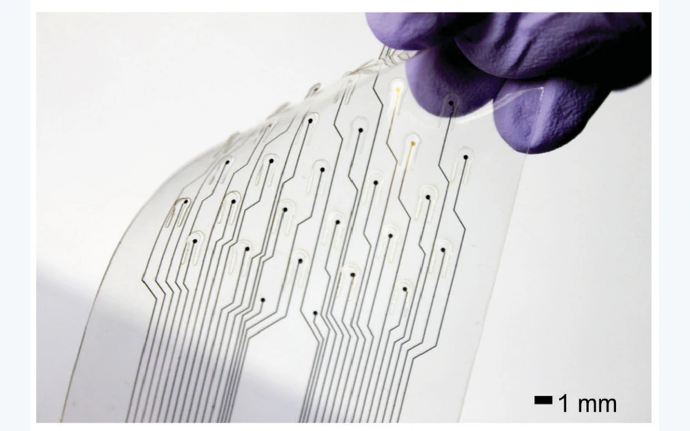
A raster image can communicate intent but should not become the production master. Controlled vector or circuit data makes site dimensions, trace widths, clearances, insulation openings, tail conductors, connector lands, and revision differences inspectable.
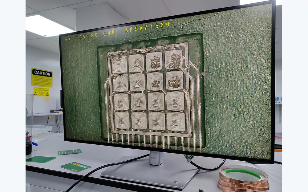
The array becomes usable only when its outside profile, holes, slots, contact openings, material zones, reinforcement, tail exit, labels, and package orientation agree with the circuit datum. Critical positions should be measurable after conversion.
Close sites, traces, dielectric, reference features, tail, connector lands, pin map, and electrical acceptance.
Name substrate, backing, adhesive zones, reinforcement, liner, labels, die cut, and approved materials.
Review print, dimensions, registration, electrical checks, interface, flexibility, handling, label, and package.
Lock artwork, materials, parts, fixtures, records, packaging, substitutions, notification, and requalification triggers.
Obtain controlled coordinates, dimensions, names, datums, orientation, and revision instead of tracing a screenshot.
Compare artwork datum, print registration, lamination, converted-layer datum, die-cut tool, fixture, and material stability.
Review ink and substrate lot, print thickness, cure, trace geometry, dielectric, conditioning, fixture contact, and test method.
Separate manufactured geometry and circuit evidence from installation, mating electronics, firmware, algorithm, environment, use, safety, and complete-system validation.
Printed contact arrays used with controlled acquisition, interpretation, and study methods.
Custom electrode geometry integrated with fixtures, connectors, and measurement hardware.
Custom circuits and converted layers produced to an OEM regulatory and device-validation plan.
The fastest review starts with controlled geometry and a clear description of the state expected at handoff.
Yes, when the artwork provides controlled site, trace, dielectric, tail and connector geometry plus materials, dimensions, tolerances, electrical tests, converted layers, packaging, and ownership boundaries.
Controlled vector or circuit data is preferred because site dimensions, trace widths, clearances, openings, conductor order, connector lands, and revisions remain inspectable.
Project-specified converted layers can be included with exact material, source, zone map, overlap, thickness, liner, handling, storage, packaging, inspection, and customer validation requirements.
Yes. JASPER can flag trace density, clearances, dielectric registration, tail geometry, converting access, material overlap, and inspection feasibility while the customer retains functional and safety design ownership.
No. It can prove released dimensions, print, continuity, resistance, isolation, interface, registration, and package state. Installation, electronics, firmware, algorithms, use, safety, clinical or research conclusions, and regulatory validation remain with the customer.
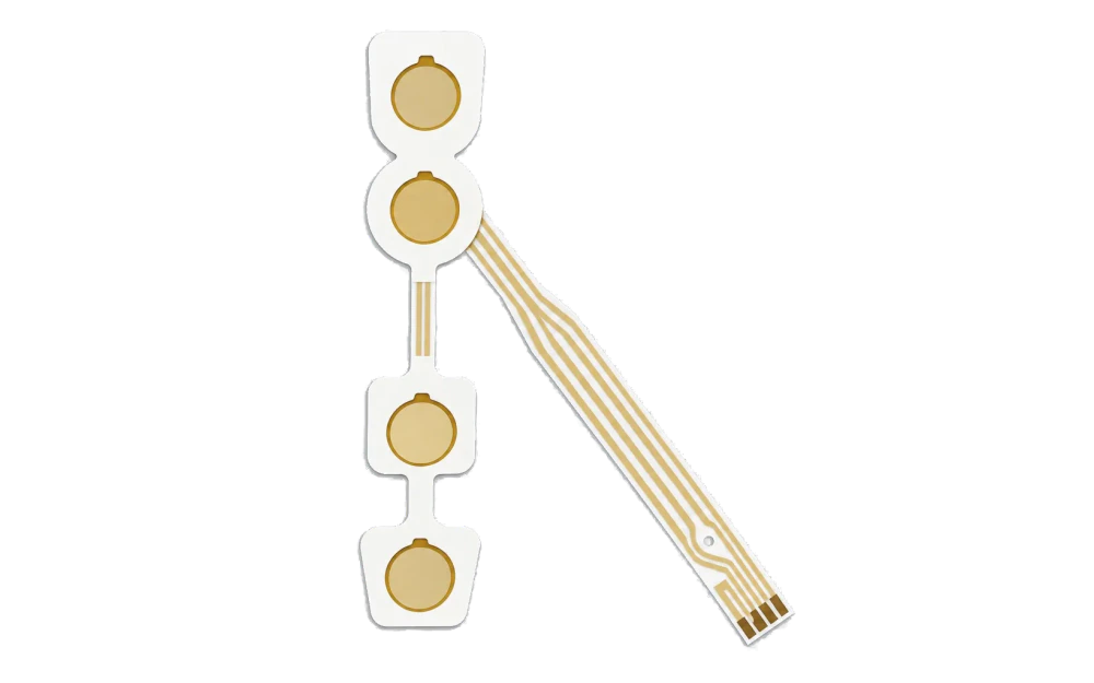
Review multi-channel neurophysiology site maps and placement features.
Review Route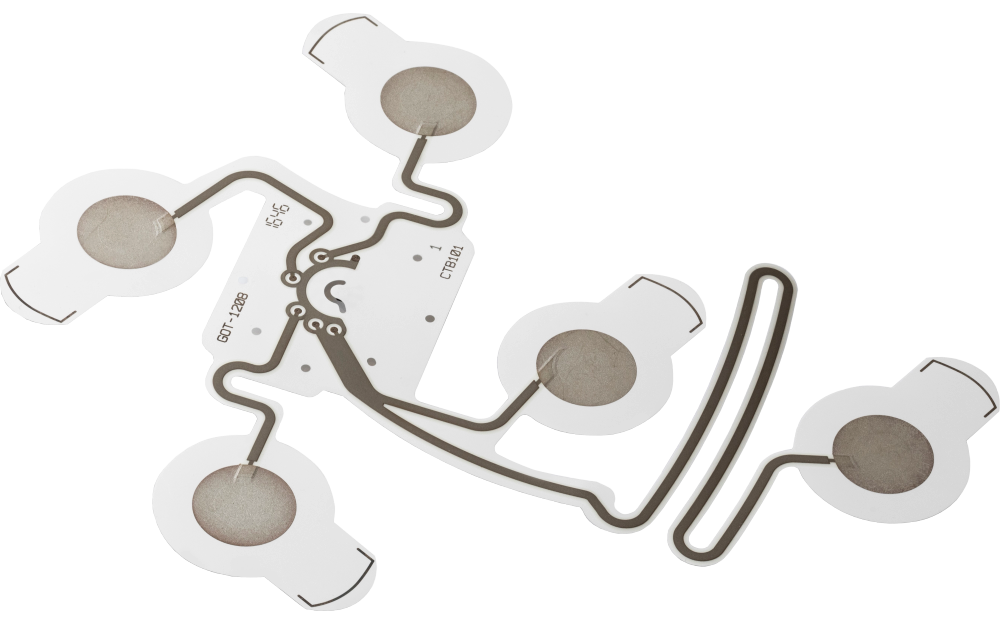
Review flexible sensing circuits with component lands and wearable mechanical zones.
Review Route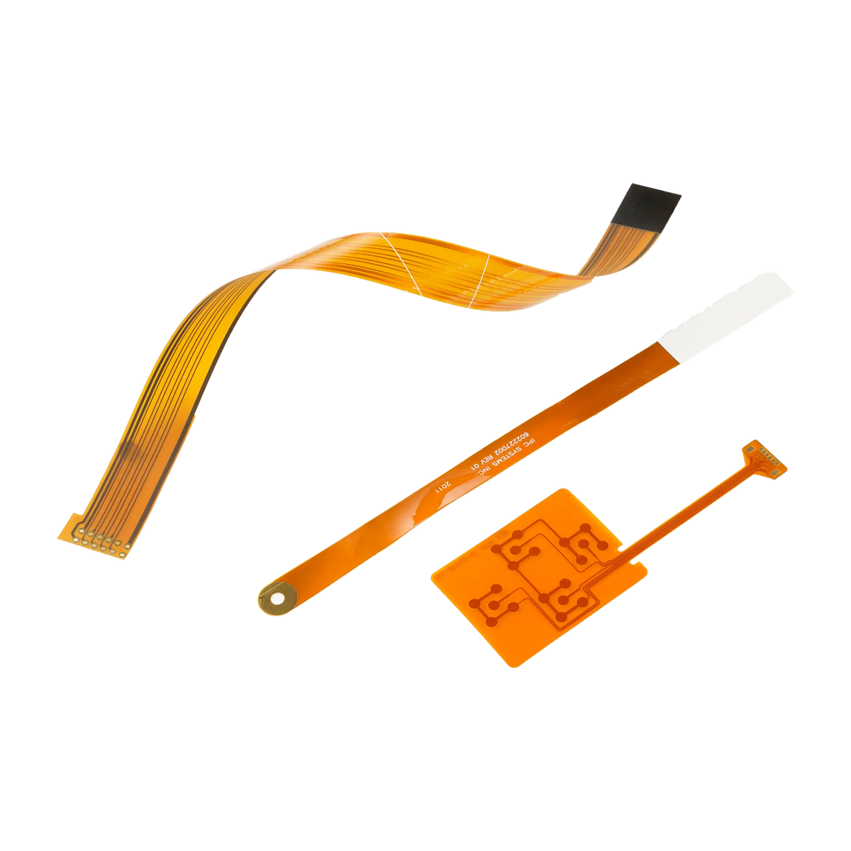
Use the printed-circuit route when converted electrode layers are not part of the supply.
Review RouteJASPER can review printed geometry, dielectric, substrate, tail, connector, converted layers, die cutting, electrical inspection, packaging, traceability, and change control.
Share the project basics. JASPER will review the stack, materials, connector, quantity, and production risks.