
Membrane switch circuit design is the work of turning a key map and host schematic into a releasable printed, FPC, or PCB circuit layer—with matrix or common-bus routing, contact geometry, dielectric crossovers, LED nets, shield termination, tail width, and a frozen pinout—before artwork leaves engineering.
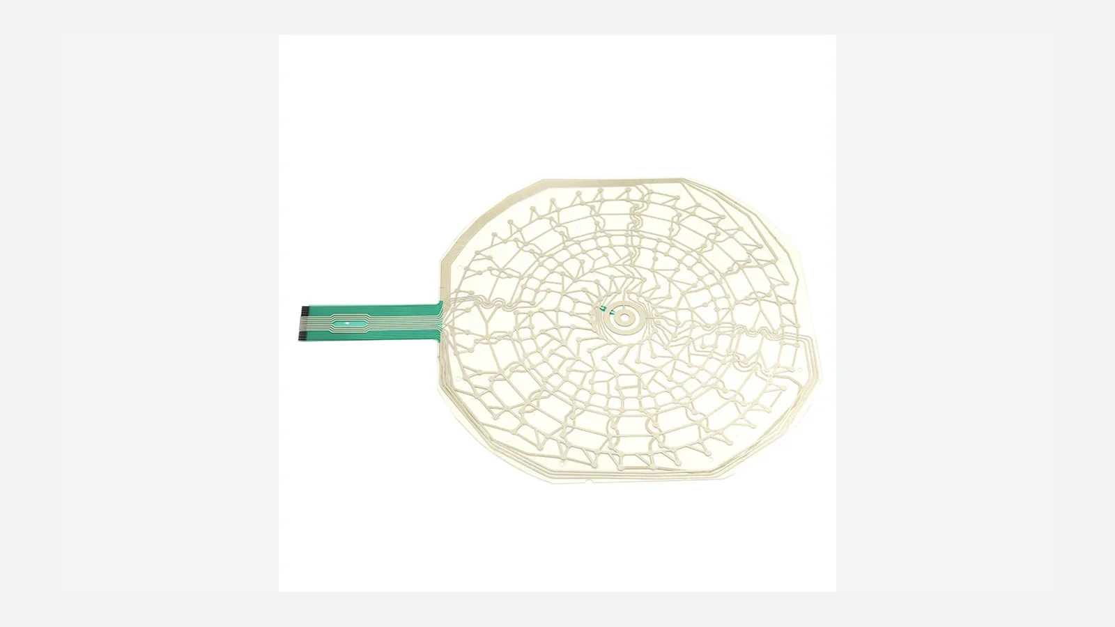
Membrane switch circuit design decides whether a keypad will scan cleanly, light the right indicators, survive the tail bend, and match the controller pinout on the first sample. This article is for OEM electronics and mechanical engineers who already know they need a custom membrane interface and now must freeze electrical architecture before screen printing or flex tooling. It covers construction choice, membrane switch matrix circuit tradeoffs, printed membrane circuit limits, LED and shield nets, and the membrane switch pinout package that manufacturing can build and test. It does not set finished-device regulatory approval, universal current ratings, or commercial terms.
For denser routing or component-heavy builds, compare PCB and FPC membrane switch constructions against a printed silver stack early—after the matrix and pinout exist, not after the first failed sample.
1. What Membrane Switch Circuit Design Actually Freezes
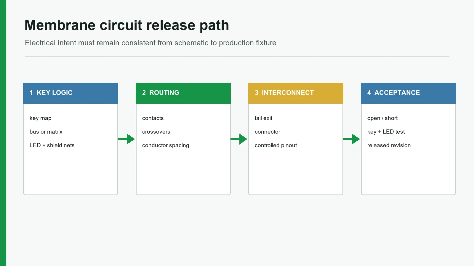
Membrane switch circuit design freezes five linked decisions at once: how keys close electrically, how those nets leave the panel, how indicators and shields share the stack, how the tail mates to the host, and how manufacturing will prove continuity before shipment. Overlay color and logo artwork matter, but they do not rescue a wrong pin map or a tail that cracks at the enclosure exit.
Treat the circuit package as a release gate, not a late drawing note. Conductive layout, termination pitch, electrical limits, force, and sealing belong in one controlled specification because a key that feels correct but opens after flex still fails.
Release sequence (use this order):
- Key map and function list — every switch, LED, shield pin, and spare net named.
- Host interface — controller type, scan method, pull-ups, LED drive polarity, ESD strategy.
- Architecture — common bus, X-Y matrix, or hybrid; dedicated nets only where required.
- Construction — printed PET silver, carbon contact treatment, copper FPC, or rigid PCB support.
- Geometry — contact pads, trace corridors, keep-outs under windows and emboss, dielectric plan.
- Tail and pinout — exit side, length, bend path, stiffener, connector family, pin 1 mark.
- Test definition — opens, shorts, key actuation, LED function, shield continuity if used.
- Artwork revision lock — one controlled pinout table shared by electrical, mechanical, and supplier.
Skip step 2 and teams often “optimize” the membrane for panel cosmetics while the MCU still expects a different scan order. Skip step 7 and first-article arguments become opinions instead of measured nets.
2. Circuit Constructions for a Printed Membrane Circuit, FPC, or PCB
A printed membrane circuit usually means silver conductive ink screen-printed on heat-stabilized polyester (PET), with optional carbon at the contact face and printed dielectric for isolation or crossovers. That stack remains the default for many sealed keypads because it stays thin, flexible, and efficient for moderate key counts. Copper flexible printed circuit (FPC) and rigid printed circuit board (PCB) constructions enter when density, bend life, current, or mounted components exceed what a practical printed-silver layout can hold.
| Construction | Typical role | Strong fit | Review carefully when… |
|---|---|---|---|
| Printed silver on PET | Key matrix traces and tails | Moderate key counts, thin sealed panels | Fine pitch, high flex cycles, higher current, dense components |
| Carbon overprint on contacts | Contact face / wear layer | Silver migration or wear risk at pads | Mating surface, force, and contamination are undefined |
| Printed dielectric | Isolation and crossovers | Multi-layer printed routing | Registration, cure, and coverage are not controlled on the drawing |
| Copper FPC | Dense routing, fine connectors, SMT parts | Tight tails, repeated flex, LED/resistor populations | Coverlay, bend radius, finish, and assembly process are incomplete |
| Rigid PCB (or PCB-backed) | Stable component platform | Heavy SMT, stiff support, complex interconnect | Enclosure clearance, sealing path, and UI stack height conflict |
the construction choice is justified by load, routing density, bend path, connector pitch, and BOM—not by habit.
“Use FPC because it is better” with no matrix density, current, or bend evidence.
Qualified manufacturers may support more than one circuit path, but the released drawing must name the selected construction. For material families beyond the circuit layer, see the membrane switch materials overview. Product-level PCB/FPC options sit on the PCB/FPC membrane switches page.
3. Common Bus vs Membrane Switch Matrix Circuit
A common-bus layout ties one side of many switches to a shared return and brings individual lines out for each key (or small groups). An X-Y membrane switch matrix circuit assigns keys to row and column intersections so the host scans intersections instead of dedicating one input pin per switch. Circuitry uses a common bus, a matrix, or a combination of the two—hybrid layouts are normal when a few keys need dedicated lines (power, safety, or high-priority interrupts) while the rest share a matrix.
| Decision factor | Prefer common bus / dedicated lines | Prefer matrix | Hybrid note |
|---|---|---|---|
| Key count vs MCU pins | Low key count, spare pins available | High key count, limited pins | Matrix for most keys; dedicated for critical nets |
| Simultaneous presses | Simple multi-key logic | Needs diode strategy or firmware policy | Document ghosting / N-key rules |
| Scan firmware | Minimal | Requires scan + debounce design | Freeze scan order in the pinout table |
| Trace density on panel | Higher pin count on the tail | Lower pin count; denser on-panel grid | Watch crossover count |
| Safety / power keys | Often dedicated | Avoid burying in a shared matrix without review | Separate early |
Topology math provides a simple example: a 4×4 keypad can leave on eight scan lines instead of sixteen dedicated key lines. Use that only as topology math—not as a claim that every product should be 4×4.
each key’s electrical identity appears in both the schematic symbol list and the graphic key map with the same name.
matrix rows and columns renumbered between sample revisions without a pinout revision letter.
Matrix routing also changes failure modes. A short between adjacent columns can create phantom keys; an open row can kill an entire bank. Design keep-outs, dielectric coverage, and test coverage around those multi-key failure patterns, not only single-switch opens.
4. Contacts, Crossovers, and Dielectric Registration
Contact geometry is the place where mechanical force becomes electrical closure. On printed constructions, the pad size, spacer opening, dome land (if used), and carbon or silver face must align in plan and in thickness. LID’s design guide stresses generous trace width, rounded corners, and clear gaps between neighboring conductors to keep resistance low and reduce stress cracking—habits that still depend on the supplier’s process window, so state targets as design intent and confirm on the approved sample.
Stack view at a key (top → bottom, typical tactile printed build):
- Graphic overlay — legends, windows, emboss.
- Optional dome retainer / adhesive — holds metal dome if used.
- Upper circuit (printed PET) — moving contact or dome contact land.
- Spacer with cutout — sets travel; defines open state.
- Lower circuit (printed PET) — static pad and routing.
- Optional shield layer — printed carbon/silver or foil (project-dependent).
- Rear adhesive / stiffener zones — mount and tail support.
Crossovers appear when two nets must cross without connecting. In a printed membrane circuit, that usually means a dielectric island under a jumper trace, registered to both artwork layers. Mis-registration creates either a short (dielectric miss) or an open (jumper miss). Put registration marks, layer revision letters, and a crossover count on the drawing so inspection is not a guess.
contact diameter, spacer opening, and dome series (if any) share one detail view.
crossovers added late in the tail neck where bend and registration risk peak.
Snaptron’s public guidance on dome lands and venting is a useful reminder that trapped air can change tactile response; vent paths may run through spacer, carrier, or board depending on the stack. Coordinate venting with circuit keep-outs so a vent slot does not slice a critical trace.
5. LED Nets and Indicator Routing
Discrete LEDs on the circuit layer serve status indication more often than full-panel illumination. Surface-mounted LEDs may be placed by pick-and-place on the circuit layer; that choice adds polarity, series resistor ownership, local thickness, and thermal path to the circuit package. Light-guide film (LGF) and electroluminescent (EL) options belong to optical design; here the circuit question is simpler: which pins drive which emitters, and can the printed or copper layer carry those nets without starving key routing.
Design rules that prevent sample loops:
- Name every LED on the key map and pinout (LED_PWR_GRN, not “D3 mystery”).
- Freeze anode/cathode orientation in a footprint note matching the LED drawing.
- Decide whether resistors live on the membrane, on the host board, or in a harness.
- Keep high-current or heat-dense parts off fragile tail necks.
- Avoid burying key traces under LED windows or perforations where rework is impossible.
Butler’s layout notes warn against routing under LEDs, windows, or perforations—treat that as risk management, not folklore. If indicator current or density climbs, move to copper FPC or a small rigid daughter board rather than forcing more silver into a crowded PET field.
LED netlist, resistor location, and window mask revision share one ECO package.
“same as last product” LED drive with a new host MCU that sources current differently.
6. Shielding and ESD Framing Without Fake Ratings
Shield layers appear when the equipment’s EMC plan needs a conductive plane near the user interface. Shield constructions include printed carbon, printed silver, and aluminum foil. Use a dedicated ground pin; an ungrounded shield can worsen EMI behavior.
| Shield approach | Typical use discussion | Termination expectation | Boundary |
|---|---|---|---|
| Printed carbon shield | Cost-sensitive ESD/EMI assist | Trace or tab to ground pin | Coverage and resistance are process-dependent |
| Printed silver shield | Higher conductivity printed plane | Dedicated ground pin | Silver cost and migration context |
| Aluminum foil shield | When foil fits the stack better than print | Ground strap or pin | Edge insulation and laminate control |
| Transparent ITO (selected windows) | Display/window regions needing transparency | Defined ground path | Optical and electrical tradeoffs |
Frame ESD with IEC 61000-4-2 as an equipment-level immunity test method, not as a sticker on a loose membrane. The membrane can contribute a shield path, a controlled spark gap strategy at the enclosure, and careful routing of sensitive scan lines—but the pass/fail belongs to the assembled product test plan. Likewise, IEC 60529 IP codes rate enclosures under defined conditions; a circuit layer alone does not “have IP67.”
shield coverage drawing + ground pin number + host chassis bond note.
“add a shield” with no ground return and no change to the pinout table.
7. Tail Geometry and Membrane Switch Pinout
The membrane switch pinout is the contract between the keypad and the host. It must list pin number, net name, function, and any no-connects—then match the physical contact side, pitch, and stiffener of the chosen connector. Common tail termination pitches include 2.54 mm, 1.27 mm, 1.00 mm, and 0.50 mm. Route the tail from an edge or inset location, not from the button area. The selected FPC connector drawing controls pitch, mating side, accepted flex thickness, and actuator style on the component drawing; that drawing remains controlling even when the membrane artwork is perfect.
Pinout drawing checklist (release only when every box is owned):
- [ ] Pin 1 mark on artwork and on the assembly drawing
- [ ] Contact side (gold fingers up/down) consistent with connector
- [ ] Pitch and conductor count match the connector series
- [ ] Net names identical across schematic, pin table, and test fixture
- [ ] LED polarity and shield ground included if used
- [ ] Spare pins labeled (spare vs reserved vs do-not-connect)
- [ ] Tail length, exit side, and bend radius path shown in the enclosure section
- [ ] Stiffener length/thickness called out for insertion
- [ ] Strain relief / adhesive keep-out at the enclosure slot
- [ ] Continuity test points accessible after lamination
Tail width is not a cosmetic margin. Narrow necks raise resistance and tear risk; overly wide tails fight the connector housing and the panel slot. Route the bend so copper or silver does not crease at a 90-degree unsupported fold during installation. For connector selection detail, use the membrane switch connectors guide after the pinout exists—not before.
one pinout table revision letter appears on schematic, membrane drawing, and fixture software.
host board already fabbed to a pin order the membrane vendor never received.
8. Electrical Targets and Test Matrix Before Artwork Release
Electrical numbers belong in the RFQ as acceptance language, not as marketing adjectives. LID’s public design guide discusses common specification practice: contact resistance often targeted in the low-tens-of-ohms class when new (literature examples use under 50 Ω) and held under a higher life-class limit (literature examples use on the order of 100 Ω), with insulation resistance in the high-megohm class (literature examples around 100 MΩ between isolated nets). Treat those figures as common RFQ discussion points until a project drawing freezes its own limits, test method, and sample size.
ASTM F1578 is a membrane-switch performance test method family frequently used to structure electrical and mechanical checks. Order tests by method and condition; do not assume a universal pass number for every industry.
| Test | Purpose | Define before tooling | Notes |
|---|---|---|---|
| Open / short scan | Catch missing nets and bridges | Fixture map vs pinout rev | Include matrix ghosting cases if relevant |
| Key actuation continuity | Prove pad/dome closure | Force or fixture method | Test on intended support if possible |
| Contact resistance | Track interface quality | Limit + method + environment | Common RFQ class only until frozen |
| Insulation resistance | Verify isolation | Limit between named nets | Humidity precondition if required by project |
| LED functional | Polarity and drive path | Voltage/current from host design | Resistor ownership stated |
| Shield continuity | Ground path integrity | Pin and coverage criteria | Only if shield is specified |
| Tail flex handling | Installation abuse screen | Bend path + cycle intent | Not a substitute for full flex life program |
| Visual registration | Crossovers, pads, windows | Overlay vs circuit fiducials | Photo standard helps |
Plan inspection with the quality and testing capability in mind: the drawing should state what “pass” means, not only that “100% continuity is required.” Ambiguous continuity language is how teams ship panels that light LEDs but leave one matrix row dead under temperature.
9. When a Printed Membrane Circuit Is the Wrong Choice
A printed membrane circuit is a poor default when any of the following is true:
- Connector pitch or pin count forces conductor density beyond stable printed registration.
- Repeated dynamic flex at the tail exceeds what the approved silver/PET stack has demonstrated on that bend path.
- Component population (many LEDs, resistors, ICs) needs copper pads and a controlled SMT process.
- Current or thermal load on indicator or power nets exceeds a conservative printed layout after engineering review.
- Repair strategy requires a replaceable rigid board rather than a laminated film stack.
In those cases, move keys to a hybrid: keep the sealed graphic overlay and switch layer where they help, and put dense electronics on copper FPC or PCB. The anti-pattern is forcing more dielectric crossovers and narrower silver into a PET field after the enclosure and MCU are already fixed. Wrong construction at artwork release is cheaper to fix than wrong construction after steel-rule dies and first-article jigs exist.
10. Project Input Package and Next Step
Before asking a manufacturer to plot circuit artwork, assemble:
- Schematic or netlist with scan method notes
- Key map matching graphic positions and names
- Membrane switch pinout table with pin 1 definition
- Connector series (or mating board photo/drawing)
- LED and shield requirements, including ground
- Enclosure section showing tail exit and bend
- Environmental and EMC intent at equipment level (not fake part-level IP/ESD stickers)
- Sample and production test expectations
Send that package for engineering review. JASPER can review schematic, pinout, and key map against printed PET, FPC, or PCB options and call out items that need a prototype before tooling. Use prototyping support when the bend path, matrix density, or LED stack is new to the product family. Send the schematic, pinout, and key map while the host board pins can still move.
Related reading: the broader membrane switch design guide for stack-level decisions outside pure circuit routing.
11. Frequently Asked Questions
What is membrane switch circuit design?
Membrane switch circuit design is the engineering work that converts a key map and host schematic into a buildable circuit layer—routing, contacts, crossovers, LED and shield nets, tail geometry, and pinout—so manufacturing can print or fabricate, assemble, and test the interface without guessing electrical intent.
How does a membrane switch matrix circuit reduce pin count?
An X-Y matrix assigns keys to row/column intersections. The host scans rows and columns instead of dedicating one input pin per key. A 4 x 4 matrix uses a 4×4 keypad leaving on eight scan lines rather than sixteen dedicated lines; real products still need a ghosting and debounce plan.
When should engineers choose a printed membrane circuit over FPC?
Choose printed silver on PET when key count, current, bend path, and connector pitch fit a thin laminated stack and the BOM is mostly switches plus simple indicators. Move toward copper FPC when density, repeated flex, fine-pitch connectors, or SMT population outgrow practical printed registration and durability.
What belongs on a membrane switch pinout drawing?
Pin number, net name, function, contact side, pitch, pin 1 mark, LED polarity, shield ground, spares, and the matching connector series. The same names must appear on the schematic, the membrane artwork, and the continuity fixture map under one revision letter.
Do membrane switches need EMI shielding?
Only when the equipment EMC plan requires a conductive plane at the interface. If a shield is used, terminate it to a defined ground pin or strap. An ungrounded shield can degrade EMI behavior. ESD verification follows equipment methods such as IEC 61000-4-2, not a free-floating switch label.
How are LEDs handled in membrane switch circuit design?
LEDs may mount on the circuit layer for status indication. Freeze net names, polarity, resistor location, and window alignment before artwork. High density or thermal load often pushes the design toward FPC or a small rigid board rather than more printed silver under the overlay.
What electrical tests should be defined before tooling?
At minimum: open/short mapping, key actuation continuity, and any LED function. Add contact resistance, insulation resistance, shield continuity, and tail handling when the RFQ requires them. Reference methods such as the ASTM F1578 family when structuring performance tests, and write numeric limits on the project drawing.
Can IP67 be assigned to the circuit layer alone?
No. IEC 60529 IP codes classify protection of enclosures under defined test conditions. Sealing is an assembly and enclosure result. The circuit contributes routing and exit details, but the IP claim needs a defined test article.
What files should be sent for a circuit design review?
Send the schematic or netlist, key map, pinout table, connector or mating-board details, LED/shield notes, enclosure section for the tail, and the intended electrical test list. That set is enough for a manufacturer to challenge matrix architecture and construction before artwork freezes.
Technical References
- Source: IPC-2223 flexible circuit design standard. Accessed 2026.
- Source: IPC-6013 qualification and performance specification for flexible circuits. Accessed 2026.
- Source: IPC-D-325 documentation requirements for printed boards and assemblies. Accessed 2026.
- Source: ASTM F1578 membrane switch contact closure cycling practice. Accessed 2026.
- Source: IEC 61000-4-2 electrostatic discharge immunity testing. Accessed 2026.
- Source: IEC 60529 enclosure protection classification. Accessed 2026.
- Source: TE Connectivity FPC connector product drawings. Accessed 2026.
- Source: Snaptron metal dome venting guidance. Accessed 2026.
- Source: IEC 60068-2-14 temperature change testing. Accessed 2026.
- Source: IEC 60068-2-78 damp heat testing. Accessed 2026.
- Source: 3M membrane switch spacer technical data. Accessed 2026.
- Source: Covestro Makrofol and Bayfol Film Selector Guide. Accessed 2026.
- Source: UL 969 marking and labeling systems scope. Accessed 2026.
- Source: RoHS Directive 2011/65/EU restricted substances scope. Accessed 2026.
- Source: REACH Regulation EC 1907/2006 chemical substance framework. Accessed 2026.
Freeze the circuit before artwork release
Send the schematic, key map, matrix logic, LED and shield nets, tail route, connector, pinout, and electrical acceptance limits.