
Circuit architecture
Release controlAssign the key matrix, LEDs, components, PCB, FPC, printed circuit, connector, and customer harness.
If it is missingFunctions are duplicated, omitted, or routed to the wrong layer.
Use a PCB or FPC circuit when the interface needs more than a simple printed-silver key matrix. The right construction depends on component mounting, connector retention, bend geometry, shielding, test access, enclosure depth, and who owns the electrical handoff.
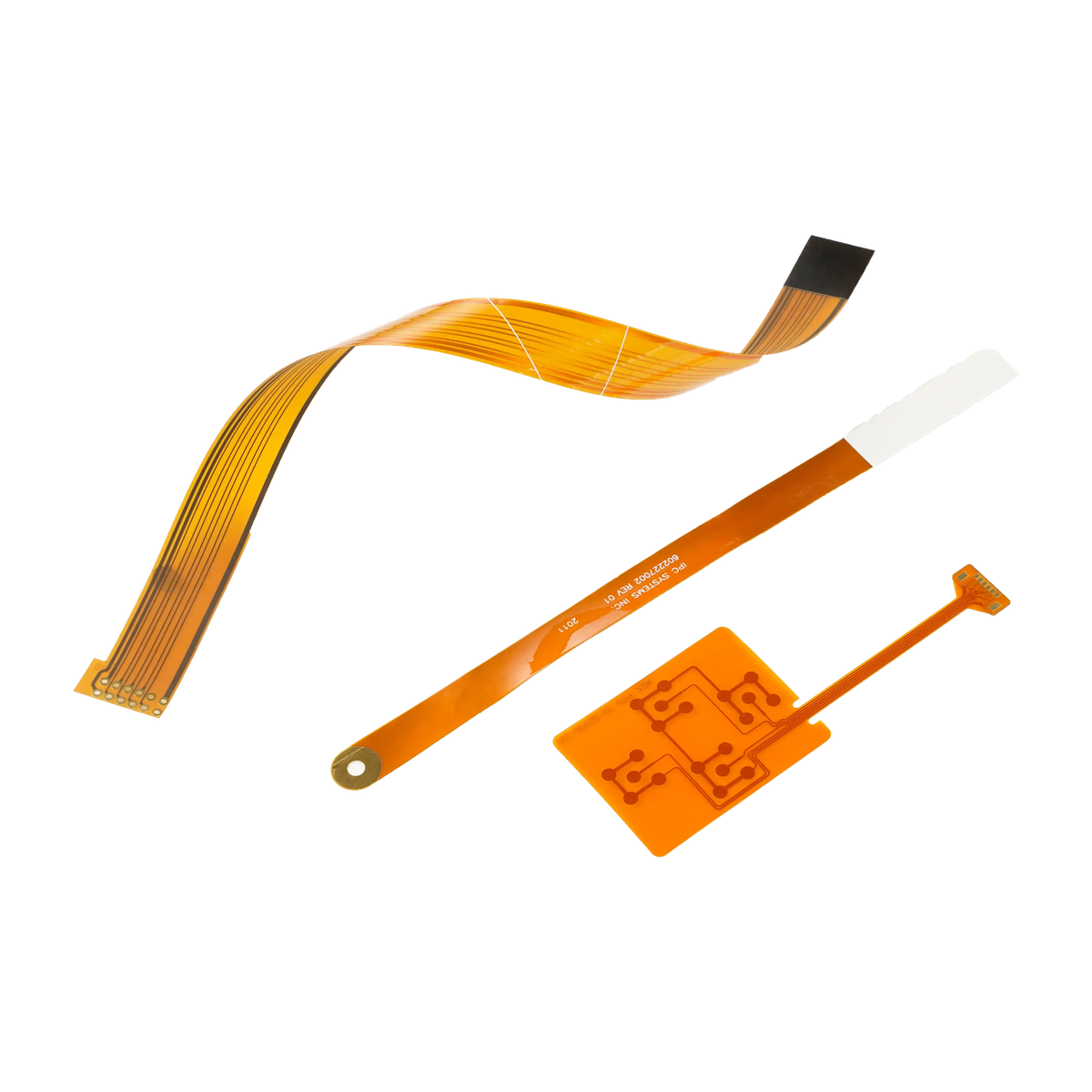
A rigid PCB is useful when switches, LEDs, resistors, connectors, or other components need mechanical support. It also gives the enclosure a stable electrical datum, but it consumes depth and needs mounting support.
An FPC keeps the interface thin and routes through narrow spaces. Its copper weight, stiffener, bend radius, connector edge, and repeated-flex expectation must be stated; a nominal outline does not define those details.
A printed silver circuit remains the lower-complexity option for many key matrices. Moving to PCB or FPC should solve a real electrical, mechanical, or assembly constraint rather than simply changing material.
Circuit files, mechanical datums, components, and the customer harness must describe the same assembly.
Assign the key matrix, LEDs, components, PCB, FPC, printed circuit, connector, and customer harness.
If it is missingFunctions are duplicated, omitted, or routed to the wrong layer.
Control board origin, holes, tail exit, stiffener edge, bend zone, connector direction, and component keep-outs.
If it is missingThe circuit passes bench test but collides with ribs, bosses, or the enclosure wall.
Release part numbers, package height, orientation, LED polarity, resistor ownership, substitutions, and marking.
If it is missingThe assembly works only after manual rework or is connected backward.
Name mating connector, pin numbering, latch direction, insertion path, retention, and harness ownership.
If it is missingThe mating cable cannot be installed or exits in the wrong direction.
Define shielding layer, ground path, chassis relationship, tail shielding, ESD path, and customer ground.
If it is missingNoise or ESD behavior changes after installation in the final enclosure.
Define continuity, resistance, LED, component, connector, and fixture checks with pass criteria.
If it is missingA basic key scan is mistaken for complete assembly approval.
Release each decision in both the electrical package and the mechanical drawing.
| Decision | Options to review | Release question |
|---|---|---|
| Circuit type | Rigid PCB, FPC, printed silver, carbon, hybrid board-and-flex, single or double sided | Which construction solves the actual routing and component requirement? |
| Components | LEDs, resistors, connectors, sensors, shielding, test pads, stiffeners, strain relief | Which items are supplied and assembled by JASPER? |
| Geometry | Thickness, holes, outline, tail exit, bend radius, stiffener, keep-outs, mounting support | Does the released geometry match the final enclosure and assembly sequence? |
| Electrical interface | Matrix, pinout, voltage, current, polarity, ground, shield, mating harness | What must be present at the customer connector? |
| Test and records | Continuity, resistance, component check, LED check, fixture output, labels, lot records | Which evidence is required before shipment? |
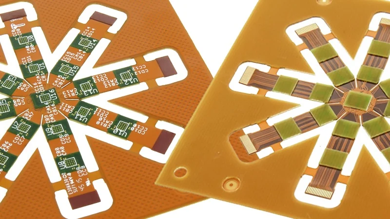
Copper can survive a designed bend and still fail at an uncontrolled crease, unsupported connector, sharp stiffener transition, or assembly pinch point. Show the installed route, not only a flat tail outline.
Assign keys, LEDs, components, rigid and flexible circuits, connector, shield, and customer harness.
Match pinout, origin, holes, tail, bend, stiffener, keep-outs, enclosure depth, and assembly direction.
Use the intended materials, copper, components, connector, adhesive, front stack, and support method.
Check fit, connector access, key scan, LEDs, components, polarity, continuity, and worst-case bend condition.
Control files, BOM, approved substitutions, test fixture, output records, labels, packaging, and change notification.
Check bend radius, stiffener edge, connector insertion, strain relief, copper damage, adhesive pinch, and shipping position.
Compare polarity, pinout, resistor ownership, component orientation, solder quality, voltage, current, and harness mapping.
Review enclosure bosses, component height, connector access, mounting support, overlay stack, and cable direction.
Trace shield coverage, ground path, tail shielding, chassis contact, ESD route, customer harness, and enclosure material.
Compact front controls with LEDs, supported connectors, controlled routing, and documented electrical checks.
Panels with status indication, shielding, robust connectors, and repeatable enclosure mounting.
Thin FPC routes through limited space with controlled bends, stiffeners, and compact connectors.
Dense key matrices, indicators, test points, and revision-controlled pinouts.
Integrated keys, LEDs, connectors, and board support for repeatable assembly.
Supported circuits, retained connectors, vibration-aware routing, and clear electrical handoff.
A Gerber or FPC outline alone does not show how the switch, connector, bend, and enclosure must work as one assembly.
Use FPC when copper conductors, tighter pitch, controlled impedance or grounding, component attachment, stiffeners, robust connector interfaces, or compact routed bends justify the additional construction. A simple key matrix may still be better served by printed silver.
A rigid PCB is usually better when components or connectors need mechanical support, when the assembly mounts to defined posts, or when test points and stable board geometry matter more than thin routing.
Yes, when the part numbers, package height, polarity, resistor ownership, voltage, current, placement, soldering, inspection, and test criteria are released.
The answer depends on copper, layer count, thickness, stiffener transition, static or repeated movement, temperature, and assembly route. Mark the bend region and expected motion so it can be reviewed against the released stack.
The project can include continuity, resistance, key matrix, LED, component, polarity, and connector-output checks when the fixture, stimulus, expected result, and record requirement are defined.
Send the mechanical outline, schematic, Gerber or FPC data if available, BOM, pinout, connector, component and LED requirements, enclosure model, quantity, and test expectations. Early files can still be reviewed before they are final.
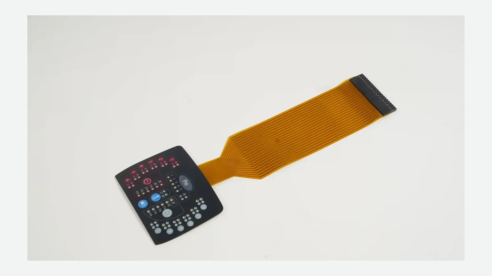
Review connector retention, pitch, orientation, mating access, and tail stiffener details.
Review Route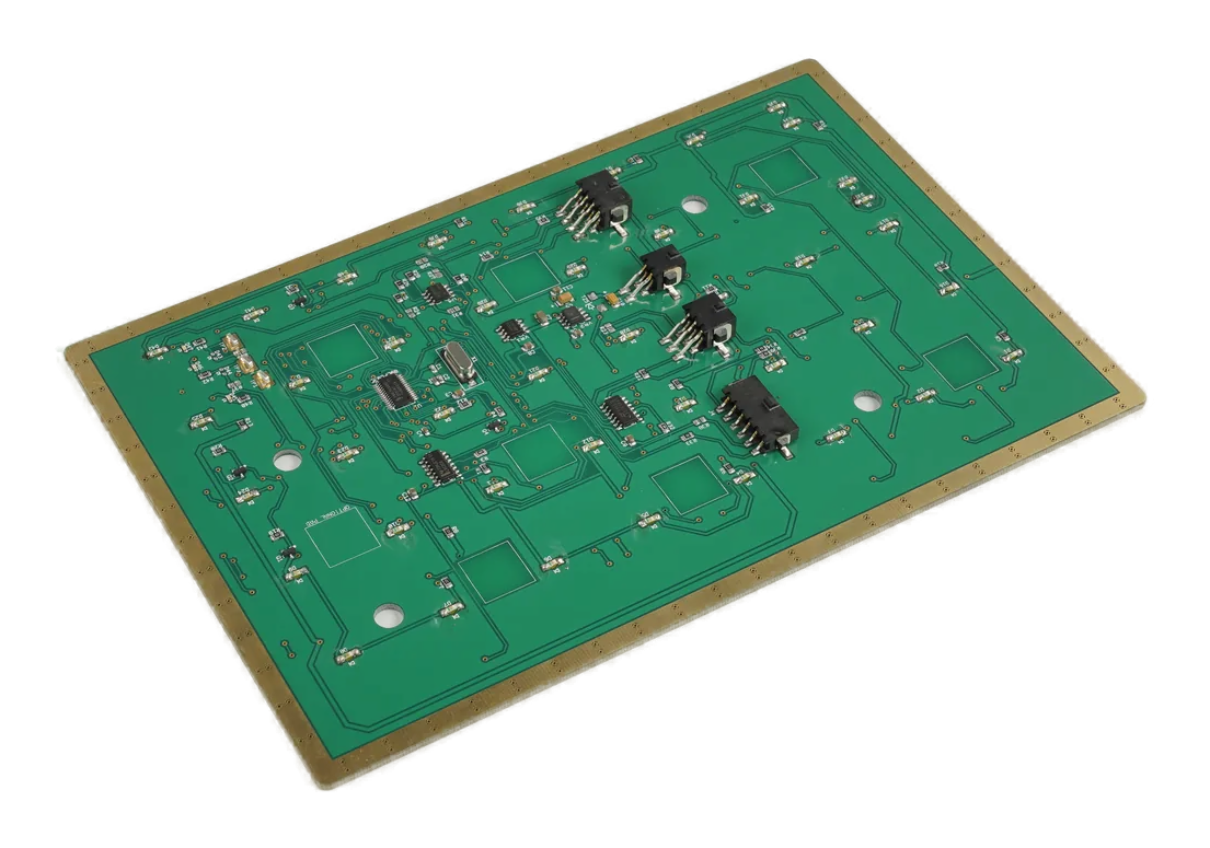
Use the broader HMI route when electronics, displays, carriers, programming, and module-level test are also required.
Review Route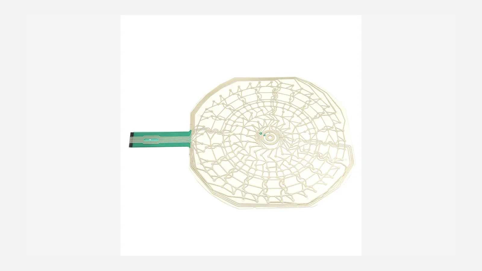
Prepare matrix, pinout, tail routing, shielding, and electrical test requirements.
Review RouteJASPER can review the overlay, switch stack, PCB or FPC, components, connector, bend geometry, enclosure, and electrical evidence before tooling.
Share the project basics. JASPER will review the stack, materials, connector, quantity, and production risks.