
Silicone keypad carbon pill resistance is not one universal material value. OEM engineers should derive an allowable installed closed-path resistance from the input circuit, then specify pill geometry, PCB contacts, applied load, test energy, sense points, environment, and lifecycle state. This guide shows electronics, mechanical, quality, and sourcing teams how to set that boundary and turn it into an acceptance plan.
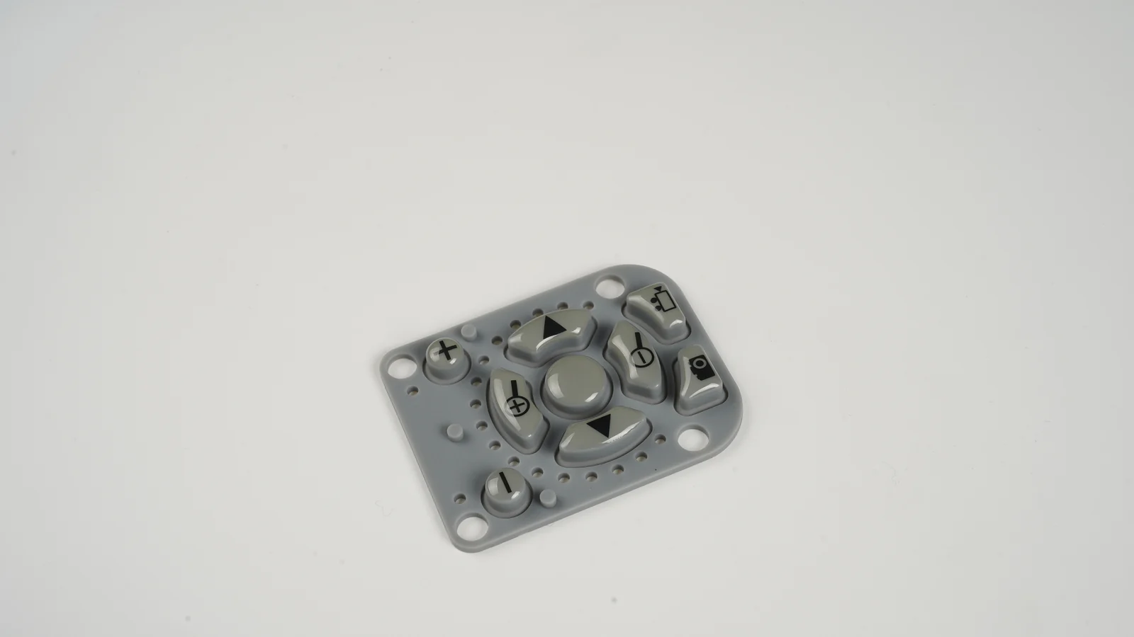
A carbon pill can measure well by itself and still fail over a production PCB. The missing variables are often the two pill-to-pad interfaces, available force, minimum overlap, surface condition, board support, and the test circuit. Those variables belong in the drawing package for conductive rubber keypads, not in an informal note added after sample failure.
One value in this guide—200 Ω maximum initial closed-contact resistance at 2.0 N applied load—is a initial worked value, not JASPER-verified data. It illustrates how to write a complete requirement. Replace it with a circuit-derived limit and verified project data before release or design release.
1. Why One “Carbon Pill Resistance” Number Fails
The phrase conductive rubber keypad resistance can refer to at least five different quantities. They are not interchangeable. The boundary matters. ASTM D991-89(2026) addresses the bulk volume resistivity of electrically conductive and antistatic rubber; it does not determine what a molded pill will measure when pressed onto a specific PCB pattern. The installed result includes material, geometry, two contact interfaces, force, surface films, and the electrical method.
| Quantity | Definition | Includes | Does not establish by itself |
|---|---|---|---|
| Volume resistivity | Bulk material property normalized for specimen geometry, usually expressed in Ω·cm | Conductive compound and defined laboratory specimen | Real pill surface, PCB pads, load, overlap, contamination, or assembly |
| Pill part resistance | Resistance through a molded pill in a defined fixture | Pill formulation, dimensions, fixture contacts, applied load | Installed two-pad current path or final housing support |
| Closed contact resistance | Resistance across the pressed pill-to-pad interface | Pill path plus both pill-to-pad interfaces | Connector, cable, long PCB traces, or controller input margin unless included intentionally |
| Total closed-path resistance | Resistance between declared system terminals while the key is pressed | Contact plus specified traces, connector, cable, protection parts, and fixture contributions | Open-state isolation or transient closure behavior |
| Open-state resistance / leakage | Isolation between the circuit nodes while the key is released | Surface leakage, residue, contamination, unintended bridges | Closed-state voltage margin |
Shin-Etsu Chemical’s June 2024 EC Series Electrically Conductive Silicone Rubber Products catalog explains volume resistivity as a geometry-normalized bulk property and identifies carbon among the conductive materials used in conductive silicone. That supplier data is useful for compound control. It is not a switch result. It cannot replace silicone keypad contact resistance measured on the production-intent pill, contact pattern, and support.
The purchasing error is to put “carbon pill: 200 Ω” on an RFQ and assume every party understands the same boundary. One supplier may measure a loose pill between fixture electrodes. Another may measure from PCB test points. A third may report continuity through a connector. All three readings can be honest while describing different electrical paths.
Decision rule: never approve a resistance value until the drawing identifies the state, terminals, mechanical load or displacement, electrical stimulus, measurement timing, environment, and lifecycle condition.
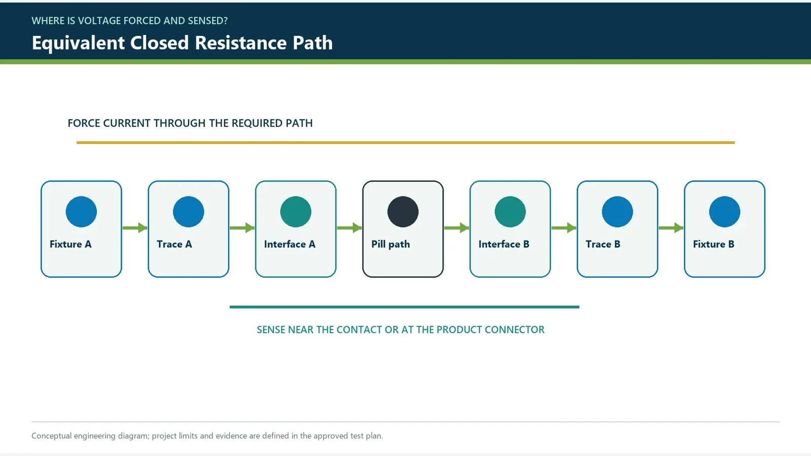
2. Model the Complete Carbon Pill Keypad Contact Path
A carbon pill keypad closes when the molded silicone web deflects and the conductive element bridges two electrically separate PCB contact regions. Epec’s silicone-keypad documentation confirms that basic architecture. Closure is only the start. The current still has to cross a complete stack, not a single ideal resistor.
Source terminal / Product trace A
PCB conductor region A
Pill-to-pad interface A
Conductive path through molded carbon pill
Pill-to-pad interface B
PCB conductor region B
Sense terminal / Product trace B
Mechanical path acting on the same interface:
Finger or actuator → Keytop → Silicone web → Pill → PCB pad → Board support → Housing
A useful diagnostic model is:
Rmeasured = Rfixture + Rtrace_A + Rinterface_A
Rpill_path + Rinterface_B + Rtrace_B
This series expression is not a promise that every term is constant or separately measurable. Elastomer deformation can change apparent contact area. Surface films can behave non-ohmically. Temperature and current can alter a low-resistance measurement. The model’s purpose is to prevent an unexplained fixture or long trace from being assigned to the pill—and to prevent the opposite mistake of removing real interface resistance from the acceptance boundary.
The sense points define what the result means. Sensing beside the PCB pad isolates more of the contact interface. Sensing at the board connector includes the routed assembly path. Measuring at an external HMI connector may include a cable and another interconnect. A silicone keypad HMI assembly can justifiably be tested at a broader boundary than a loose keymat, but the drawing must say which boundary applies.
the schematic, pad artwork, section drawing, and test specification mark the same source and sense terminals.
a resistance limit appears next to the pill diameter while the actual test is run through an unspecified matrix connector.
3. How to Set a Silicone Keypad Carbon Pill Resistance Limit
The correct limit starts at the controller input, not at a compound catalog. For a simplified active-low digital input with a pull-up resistor:
VCC
Rpull-up
Input node
Rclosed_total ← keypad contact plus every included series element
Ground
Ignoring leakage and protection networks for the first calculation:
Vlow = VCC × Rclosed_total / (Rpull-up + Rclosed_total)
Rclosed_total ≤ Vlow_target × Rpull-up / (VCC − Vlow_target)
Worked digital-input budget
Assume an early design uses VCC = 3.3 V, a 10 kΩ pull-up, and an internal design target of Vlow ≤ 0.60 V. The idealized total closed-path ceiling is:
Rclosed_total ≤ 0.60 × 10,000 / (3.30 − 0.60)
Rclosed_total ≤ 2,222 Ω, approximately
That 2.22 kΩ is not yet a contact specification. The electronics team must reserve margin for the actual input-low threshold over temperature, pull-up tolerance, supply tolerance, leakage, cable and connector resistance, ESD/filter components, ground offset, noise, scan settling, and measurement uncertainty. If the project allocates 0.72 kΩ to those effects, the worked contact budget becomes 1.50 kΩ. That allocation is an example, not a universal safety factor.
The worked drawing line below is intentionally much tighter than the illustrative 1.50 kΩ functional budget:
Worked engineering requirement: Set initial closed-contact resistance at 200 ohms maximum under 2.0 N applied load, measured across the declared PCB test points after the declared dwell. Confirm the final limit from project characterization and circuit margin.
Why leave margin? A digital input only needs enough electrical margin to cross its threshold, but the production requirement must also accommodate sample variation, aging, contamination, fixture uncertainty, and fault detection. The project may choose a different allocation after characterization. It should not promote the worked 200 Ω line into a guaranteed value merely because it is familiar.
Matrix and analog circuits need different budgets
A scanned matrix adds driven-line state, pull-up or pull-down tolerances, inactive-line behavior, diode drops where fitted, connector paths, scan rate, and settle time. Firmware debounce may reject short transitions. It cannot repair a closed voltage that never reaches the controller threshold or a key that opens for longer than the debounce window.
An analog or resistance-coded keypad is more restrictive. Carbon-pill variation becomes part of the measured code, so the budget must include resistor tolerance, ADC error, reference error, leakage, cable effects, temperature, and contact drift. A contact acceptable for a digital GPIO may be unsuitable in a narrow analog decision window.
A carbon pill should not directly switch a motor, solenoid, heater, or high-current lamp merely because a handheld meter shows closure. Load current, voltage drop, self-heating, transient energy, duty cycle, and fault behavior need separate qualification. Using the keypad as a logic input with a suitable driver is often the safer architecture.
| Circuit use | Start with | Contact decision boundary | Main failure if copied from another design |
|---|---|---|---|
| Digital input | Worst-case VIL, pull-up/down, leakage, supply, temperature | Total closed path with voltage margin | Input remains above valid-low threshold |
| Scanned matrix | Drive/sense states, timing, isolation parts, cable path | Complete selected row-column route | Unstable or late detection during scan window |
| Resistance-coded input | ADC bins, reference, resistor tolerance, drift | Contact contribution to worst-case code separation | Adjacent key codes overlap |
| Significant load switching | Current, transients, heating, fault energy | Qualified switch architecture, not continuity alone | Contact heating, unstable drop, or damage |
4. Eight Criteria for Specifying Conductive Rubber Keypad Resistance
The following criteria convert an electrical target into a controlled interface. Each is evidence that the design can move toward sample approval. Each identifies an assumption that can invalidate an otherwise credible resistance reading.
4.1 Name the resistance quantity and terminals
The first drawing note should answer, “Resistance of what, measured between where?” A material volume-resistivity requirement can control incoming compound. A pill fixture can screen a molded conductive element. An installed contact test can assess the two interfaces and pad geometry. A connector-to-connector test can verify the supplied assembly. Those are four legitimate controls, but they serve different purposes.
ASTM D991 and the Shin-Etsu EC Series catalog support the distinction between bulk material behavior and installed contact behavior. Neither source supplies a universal keypad limit. If the project needs both compound control and an assembly result, place them in separate specification rows with separate methods.
the requirement says “closed contact,” “total path,” or “volume resistivity,” identifies source/sense terminals, and specifies open or pressed state.
the BOM contains one unlabeled resistance number and the inspection plan calls it alternately material resistance, pill resistance, and keypad resistance.
4.2 Derive the limit from the circuit
A circuit-derived budget gives the number a reason to exist. The electronics owner should document the worst-case input threshold, supply, pull component, leakage, protection network, cable, connector, temperature, timing, noise, and design margin. The remaining allocation belongs to the contact boundary that the supplier can control and test.
The budget also prevents needless over-specification. Demanding the lowest available resistance may force a different material, pad, test method, or contact architecture without improving controller performance. Conversely, accepting a broad catalog range may leave too little voltage margin after temperature and series losses are added.
a worst-case calculation links the contact limit to a schematic revision and names the margin reserved for non-contact effects.
the limit was copied from a prior keypad with a different supply, pull-up, matrix route, connector, or ADC scheme.
4.3 Control pill diameter, position, retention, and applied load
Pill diameter is not the same as electrical overlap. The conductive element must bridge both separated contact regions at the worst combination of molding position, PCB position, housing clearance, key tilt, and edge actuation. Pill thickness also affects rest gap, first touch, contact load, available overtravel, and the conductive path.
The useful result is measured in a defined stable region of the key’s force-displacement curve. An unspecified finger press can hide a key that closes only near hard bottoming. Too little travel can create intermittent contact; excessive displacement can overload the web, pill edge, PCB, or backing support. Epec’s design guidance treats force, travel, geometry, and resistance as separate characteristics because one nominal value does not control the others.
Key travel → First physical touch → First electrical closure
Stable closed region → Intended overtravel → Hard stop
pill outline, thickness, positional tolerance, retention, key force/displacement endpoint, dwell, center press, and required edge presses are on controlled documents.
inspection applies “normal hand pressure,” or checks only a nominal center press with no minimum overlap analysis.
4.4 Design the PCB contact geometry and support with the pill
The pad must provide two conductors that the pill bridges without an unintended released-state short. Split pads, interdigitated fingers, center-and-ring patterns, and segmented contacts create different current paths and tolerance sensitivities. No pattern is universally superior.
| Pad concept | Useful design reason | Questions to close before approval |
|---|---|---|
| Split pads | Simple geometry and trace routing | Does minimum pill overlap reach both halves during center and edge presses? |
| Interdigitated fingers | Multiple parallel contact zones inside a compact footprint | Are finger width, gap, finish, contamination, and fabrication variation controlled? |
| Center and ring | Radial tolerance around a center conductor | Does tilt still contact both regions without released-state bridging? |
| Segmented / curved | Fits noncircular keys or local routing | Is the current path stable under partial contact and rotation? |
| Printed PET or FPC contact | Flexible circuit integration | Are ink surface, cure, support, flatness, and environmental behavior qualified? |
Pad artwork should show conductor dimensions, gap, solder-mask relationship, vias and trace entries, flatness, final contact surface, keepouts, and common datums. The PCB or flexible circuit needs a controlled reaction surface. If it deflects away from the pill, force, travel, overlap, and resistance change together.
worst-case tolerance analysis covers pill-to-pad location, both conductor regions, board support, housing locators, and edge loading.
the pill is located from a rubber outline, the PCB pad from an unrelated housing feature, and no assembled tolerance chain connects them.
4.5 Treat surface condition and contamination as electrical variables
Contact finish names do not describe the whole interface. The drawing should control the final contact-area build, permitted surface condition, solder-mask edge, flatness where relevant, cleaning, handling, packaging, storage, prohibited rework, and supplier-change notification.
Shin-Etsu’s EC Series handling guidance tells users to keep mating surfaces clean and avoid dirt, moisture, oil, solvents, and other contamination. For a keypad interface, the risk list can also include fingerprints, molding or release residue, silicone oil, coating overspray, print or laser debris, flux, adhesive particles, fibers, condensation residue, and housing lubricant.
Do not scrape, polish, or solvent-wipe a failed contact before recording the as-found state. That action can remove the film or debris that caused the failure and can change the pill or finish. An emergency cleaning method is itself a process change requiring compatibility and life validation.
the contact area has a documented build, approved cleaning and handling route, protected packaging, residue controls, and an as-found failure-analysis rule.
operators use any available solvent until the reading passes, with no record of the original resistance or surface condition.
4.6 Match the measurement method to the question
Two-wire and four-wire measurements are not quality tiers. They measure different boundaries. The Tektronix/Keithley Low Level Measurements Handbook explains that four-wire or Kelvin sensing removes voltage drop in leads between the source and sense points. It does not remove the two pill-to-pad interfaces. Those remain the subject of an installed contact test.
IEC 60512-2-1:2002 defines a millivolt-level contact-resistance method for electromechanical components. Its low-energy principle seeks to avoid electrical breakdown of insulating films. A keypad is not automatically an IEC connector, so the parties must approve applicability, the licensed method, and any deviations. The same distinction appears in Keithley’s dry-circuit guidance: excessive test energy can alter a surface film and report a lower resistance than the undisturbed interface presented.
| Method | What it includes | Best used when | Must be declared |
|---|---|---|---|
| Two-wire static | Leads, fixture, traces, contact, and other series elements | Total assembly path is the requirement and fixture contribution is stable and small versus the limit | Terminals, lead compensation/check, load, dwell, voltage/current |
| Four-wire / Kelvin static | Voltage between sense points while separate leads source current | Lead and fixture drop would consume meaningful resistance budget | Source and sense points, current, polarity, load, dwell |
| Low-level / dry-circuit | Contact under limited electrical energy | Characterizing the undisturbed interface film | Applied limits, standard/method, instrument range, timing |
| Functional circuit test | Actual or representative product voltage, current, thresholds, timing | Proving the complete input works as used | Schematic revision, supply, pull network, scan/debounce, pass state |
| Dynamic waveform test | Voltage/current/resistance versus force or displacement and time | Detecting bounce, brief opens, delayed closure, unstable edge press | Bandwidth, sample rate, thresholds, event window, actuation profile |
the method names source/sense nodes, force or displacement, dwell, voltage, current, polarity, range, sample rate, environment, calibration, fixture checks, and uncertainty.
“check continuity with a multimeter” is the entire acceptance instruction.
4.7 Define dynamic behavior and lifecycle states
A static value after a long hold can miss delayed closure, short opens, resistance spikes, multiple transitions, edge instability, and incomplete release. Dynamic testing should synchronize force or displacement with electrical channels when those failure modes matter.
Time-aligned channels
Force or displacement
Contact voltage
Contact current
Calculated resistance
Controller input state
Cycle count alone is not a duty profile. The plan should name the keys cycled, center or edge loading, force/displacement endpoint, cycle rate, dwell, complete release, powered state, environment, periodic measurements, rest intervals, and failure definition. A fast unpowered center press can create a different wear path from a slow gloved edge press in the installed enclosure.
| Acceptance state | Required evidence | Decision it supports |
|---|---|---|
| Initial molded sample | Pill location and surface; force/travel; static and dynamic closure | Basic design feasibility |
| Decorated and assembled sample | Same measurements with coatings, PCB, housing, preload, connector, and support | Stack interaction |
| Qualification | Multiple keys, cavities/lots, environment, cycling, and fixture repeatability | Release of design and process |
| Production lot | Defined sample or full test; open/short; visual; resistance/functional check | Shipment control |
| Post-environment | Closure, release, resistance, corrosion/contamination, physical inspection | Exposure-related change |
| Post-life | Distribution and drift, intermittent events, force shift, wear, disassembly | Duty-profile durability |
| Change qualification | Affected tests after material, pad, finish, tool, process, supplier, or fixture change | Prevention of silent interface changes |
initial and aged limits, per-key or key-group treatment, intermittent-event criteria, sample quantity, failure action, retest policy, and raw-data retention are explicit.
a single initial reading and an unconditioned cycle count are used to claim life across every key and environment.
4.8 Set the supplied boundary and failure-analysis ownership
If the shipment is a loose silicone keymat, the final PCB contact finish, board support, housing compression, connector, and controller threshold remain partly or entirely outside the keypad supplier’s control. If the shipment is an HMI module, a broader connector-to-connector functional boundary may be practical. Neither arrangement removes the need to define responsibilities.
The project should assign ownership for the schematic, pad artwork, board fabrication, cleaning, housing support, keypad and circuit alignment, fixture, firmware thresholds, environmental profile, lifecycle test, raw data, and failure analysis. JASPER’s quality testing route may support a project plan, but that page is not evidence that a specific Kelvin, dry-circuit, dynamic, or lifecycle method has already been approved for this product.
a responsibility matrix connects every interface and acceptance record to an organization, drawing revision, and change-notification rule.
a failed assembled key is automatically assigned to the rubber part before the PCB, support, test energy, sense points, and housing preload are checked.
5. Run a Seven-Step Carbon Pill Keypad Approval Process
A useful process moves from circuit need to released evidence. It does not begin by asking a supplier for its lowest resistance grade.
Step 1 — Freeze the electrical decision threshold
Release the input schematic, controller threshold data, supply and pull-component tolerances, leakage, protection/filter network, timing, temperature range, and design margin. Calculate the maximum total path, then allocate the contact portion.
Step 2 — Define the installed geometry
Provide the pill outline and location, key force/displacement curve, PCB contact artwork, final surface, board support, housing section, datums, and tolerance chain. Include center and required edge/corner presses.
Step 3 — Write the measurement method
Choose two-wire or four-wire based on the required boundary. State low-level characterization and functional testing separately where both are needed. Record electrical stimulus, source/sense points, mechanical endpoint, dwell, timing, environment, fixture checks, calibration, and uncertainty.
Step 4 — Approve a production-intent sample
Install the molded keypad on the intended PCB or a controlled production-equivalent contact coupon and representative support. Document substitutions. A loose-pill measurement can support incoming control, but it cannot approve the installed interface.
Step 5 — Characterize variation before setting final limits
Compare keys, positions, mold cavities, material lots, PCB lots, center/edge presses, fixtures, temperatures, and relevant exposures. Use distributions and raw traces; do not average away a failed high-use key. Replace the initial 200 Ω at 2.0 N example only after the project has enough evidence to set a defensible initial and aged window.
Step 6 — Qualify environment and duty profile
Cycle the keys that represent real use, with declared load, rate, dwell, release, powered state, environment, and inspection intervals. Include post-test disassembly when wear, residue, retention, or pad damage must be identified.
Step 7 — Release production controls and change rules
Tie the approved values to keypad, pill, compound, mold, cavity, PCB artwork, finish, support, fixture, software threshold, and test-method revisions. Define sampling or full test, traceability, failure action, retest, and the changes that trigger requalification. Prototyping and sample validation should close named questions, not create an attractive sample with undefined approval status.
Sample approval matrix
| Approval item | Minimum evidence | Typical owner | Release blocker |
|---|---|---|---|
| Electrical budget | Worst-case calculation and schematic revision | Electronics Engineering | No threshold margin allocation |
| Pill and force path | Drawing, force/displacement trace, center/edge condition | Mechanical / Keypad Engineering | Closure only near hard stop |
| Pad and support | Artwork, finish, flatness/support, tolerance analysis | PCB / Mechanical Engineering | Minimum overlap not demonstrated |
| Measurement system | Method, fixture drawing, calibration, short/open checks, uncertainty | Test / Quality Engineering | Fixture contribution unknown |
| Dynamic closure | Time-aligned trace and event criteria where required | Test / Firmware Engineering | Brief opens hidden by slow meter |
| Environment and life | Duty profile, intervals, initial/final distributions, disassembly | Reliability Engineering | Cycle count without load/environment definition |
| Production release | Control plan, sampling, traceability, change notification | Quality / Supplier Quality | Approved sample not tied to revisions |
6. When a Carbon Pill Is Not the Best Contact Choice
A carbon pill is not the default for every silicone key. Reject or reconsider the construction when the contact budget, load, geometry, environment, or service boundary cannot be qualified with adequate margin.
| Project condition | Why the carbon pill may be wrong | Architecture to evaluate |
|---|---|---|
| Very low or tightly controlled contact resistance | Elastomer and interface variation may consume the budget | Metal pill, metal dome, electromechanical switch |
| Significant current through the key | Voltage drop, heating, and fault energy need a rated switching element | Logic input plus driver; rated sealed switch |
| Narrow analog code spacing | Contact drift can reduce ADC decision margin | Separate switch matrix, digital encoder, different sensing architecture |
| Insufficient footprint for two-pad overlap | Tolerance and edge presses may not bridge both conductors reliably | Larger key/contact, revised pad, alternate switch |
| Uncontrolled exposed contact environment | Films, condensation, oils, or particles can dominate the interface | Sealed switch or protected internal contact system |
| Unstable PCB/FPC support | Deflection changes force, travel, and resistance together | Add support or choose a self-contained switch |
| Need for crisp metal snap behavior | Conductive elastomer may not provide the required force signature alone | Metal dome keypad or dome-over-circuit stack |
| Field-replaceable independent switch | Molded keymat and PCB interface may be too integrated | Discrete sealed switch module |
Disqualifying release blockers include: no circuit budget; no declared terminals; no minimum overlap analysis; contact tested only with finger pressure; board support omitted; unapproved solvent recovery; functional and low-level results mixed; cycle count without duty profile; open-state behavior ignored; or a supplier unwilling to record the compound, pill, pad, fixture, and lot revisions that produced the approved data.
7. Carbon Pill Drawing and RFQ Input Checklist
The RFQ should ask for an engineering response to a controlled package. It should not ask the supplier to guess the product threshold from the words “low resistance.” A broader silicone rubber keypad design guide can cover key geometry, web, legends, coatings, and enclosure integration; the list below focuses on the contact interface.
Electrical inputs
- input schematic and controlled revision;
- supply, threshold, pull-up/pull-down, leakage, and temperature tolerances;
- matrix drive/sense states, scan rate, settle time, and debounce behavior;
- maximum total closed-path resistance and allocated contact budget;
- open-state resistance or leakage requirement;
- source/sense terminals, test voltage/current, polarity, range, dwell, and timing;
- low-level, functional, and dynamic test purposes;
- powered or unpowered lifecycle condition.
Pill, key, and loading inputs
- approved compound or supplier-control route;
- pill outline, thickness, position, retention, surface, and orientation;
- key force-displacement curve and tolerance;
- first touch, first closure, stable region, overtravel, and hard stop;
- center and edge/corner press locations;
- high-use key groups, mold cavity, lot, and change-control requirements.
PCB, FPC, or PET contact inputs
- pad artwork, dimensions, gap, and minimum overlap;
- conductor and final contact-area surface;
- solder-mask, via, trace, component, and raised-feature keepouts;
- local flatness, backing support, board bow, and housing section;
- common datums, locators, and assembled tolerance chain;
- cleaning, handling, storage, packaging, rework, and supplier-change controls.
Validation and production inputs
- initial, assembled, post-environment, and post-life acceptance states;
- sample quantities, keys, cavities, lots, fixtures, and stations;
- measurement-system analysis, calibration, and uncertainty requirements;
- waveform and summary-data retention;
- environment, cleaner, oil, humidity, dust, condensation, or other exposures;
- lifecycle profile and inspection intervals;
- failure analysis, retest, sampling/full-test, and change-qualification rules;
- loose keymat or assembly-level supplied boundary.
8. Frequently Asked Questions
What resistance should a silicone keypad carbon pill have?
There is no universal silicone keypad carbon pill resistance. Calculate the maximum closed path from the controller threshold, supply, pull network, leakage, tolerances, temperature, series elements, timing, and margin. Allocate part of that limit to the installed pill-to-pad contact, then verify initial and aged distributions at declared load and test conditions.
Is conductive rubber keypad resistance the same as material volume resistivity?
No. Volume resistivity is a bulk-material property normalized for specimen geometry under a defined method such as ASTM D991. Installed conductive rubber keypad resistance also includes pill dimensions, two pill-to-pad interfaces, PCB geometry and surface, overlap, force, contamination, timing, and the chosen source/sense points.
Should silicone keypad contact resistance be measured with two wires or four wires?
Use two wires when the required result is the complete assembly path and lead/fixture contribution is stable and small versus the limit. Use four-wire/Kelvin sensing when those drops must be excluded. Both methods still require declared terminals, contact load, dwell, electrical stimulus, environment, and lifecycle state.
Why can test voltage or current change the measured contact resistance?
A pill-to-pad interface can contain films and non-ohmic microcontacts. Excess test energy may disturb a film or heat the device, producing a result that differs from the undisturbed interface. Separate low-level or dry-circuit characterization from the actual product functional test, and record both methods when both questions matter.
How do pill diameter and PCB pad geometry affect resistance?
Diameter matters through minimum electrical overlap, not appearance alone. The pill must bridge both separated pad regions under molding, PCB, housing, and actuation tolerances. Split, interdigitated, ring, and segmented contacts create different paths; validate each with the production pill, finish, support, center press, and required edge presses.
Can contamination raise carbon pill keypad resistance?
Yes. Dirt, moisture, oil, fingerprints, molding residue, coating debris, flux, adhesive particles, condensation residue, or lubricant can alter one or both contact interfaces. Record the as-found failure before cleaning, use only an approved method, and requalify any new solvent, wipe, packaging material, or handling process.
Does firmware debounce fix a high-resistance or intermittent contact?
No. Debounce can reject brief transitions only when the closed voltage still crosses the valid input threshold and interruptions stay inside the algorithm’s timing window. It cannot recover missing voltage margin, a key that closes only at hard bottoming, long opens, unstable edge contact, or incomplete release.
When should a design use a metal dome or another switch instead of a carbon pill?
Evaluate another architecture when the circuit needs very low or tightly controlled resistance, significant current, narrow analog accuracy, a smaller footprint than the tolerance chain permits, a sealed field-replaceable element, or operation over an uncontrollable exposed contact surface. Each alternative still needs its own force, surface, bounce, sealing, and life validation.
9. Submit the Resistance and Contact Package
A useful carbon-pill review starts with the input schematic and resistance budget, then adds the keypad/pill drawing, PCB contact artwork, housing and support section, force curve, environment, duty profile, supplied boundary, and acceptance method. JASPER can be considered alongside other qualified keypad and HMI sources once those inputs are controlled; the correct outcome may be a carbon pill, a different contact architecture, or a change to the controller input.
Submit the resistance and contact package with approved limits and open engineering inputs identified. Ask the reviewing team to return a written matrix that separates material control, installed geometry, measurement method, sample qualification, production acceptance, change control, and failure-analysis ownership.
Technical References
- Source: Shin-Etsu Chemical EC Series Conductive Silicone Rubber Products, June 2024. Accessed 2026.
- Source: ASTM D991-89(2026) Conductive Rubber Volume Resistivity. Accessed 2026.
- Source: Tektronix and Keithley Low Level Measurements Handbook, Seventh Edition. Accessed 2026.
- Source: IEC 60512-2-1:2002 Contact Resistance Millivolt-Level Method. Accessed 2026.
- Source: Shin-Etsu Polymer Contact Elements for Keypads. Accessed 2026.
- Source: IEC 61020-1:2019 Electromechanical Switch Framework. Accessed 2026.
- Source: ASTM F1578-24 Membrane Switch Contact Closure Cycling. Accessed 2026.
- Source: ISO 23529:2016 Rubber Test-Piece Conditioning. Accessed 2026.
- Source: ASTM D991-89(2026). Accessed 2026.
- Source: Shin-Etsu Chemical’s June 2024 EC Series Electrically Conductive Silicone Rubber Products catalog. Accessed 2026.
- Source: Epec’s silicone-keypad documentation. Accessed 2026.
- Source: The Tektronix/Keithley *Low Level Measurements Handbook. Accessed 2026.
- Source: IEC 60512-2-1:2002. Accessed 2026.
Review the keypad construction before tooling release
Send the drawing, key geometry, force targets, contact stack, artwork, housing, environment, and approval plan for a construction-specific review.