
Projected capacitive touch panel technology places a transparent electrode matrix behind an insulating cover lens, measures local capacitance changes, and converts the resulting signal map into one or more touch coordinates.
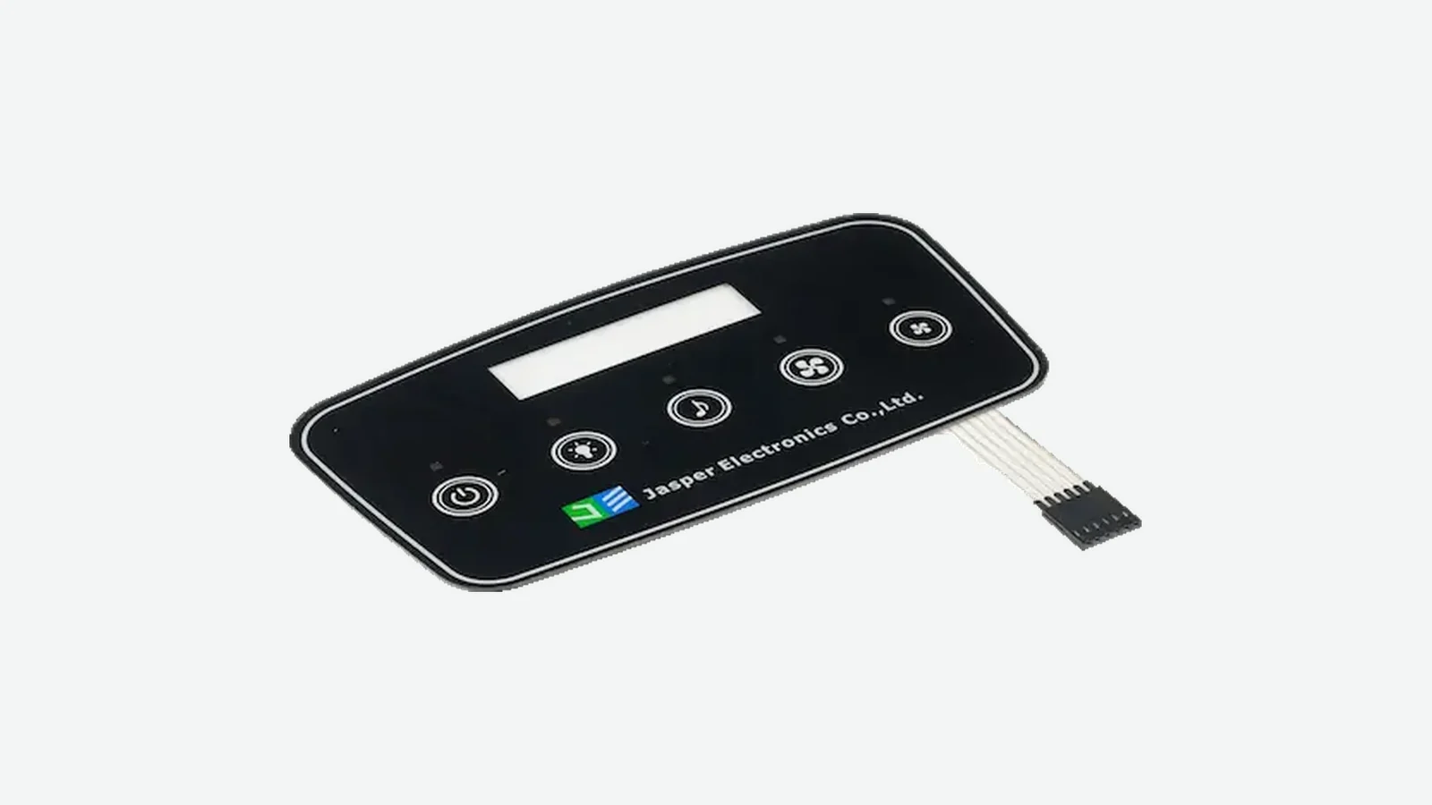
A PCAP touch panel is usually the right starting point when an OEM needs light-touch input, a durable glass front, and multi-touch coordinates. It is not a stand-alone performance guarantee. The cover lens, projected capacitive sensor, controller, display, bonding, grounding, enclosure, and host interface act as one electrical system. This guide shows device engineers and sourcing teams how that system works, what must be specified, and where panel design ends and finished-device validation begins. It does not provide controller code or claim that one construction fits every glove, liquid, EMC, or safety requirement.
What a projected capacitive touch panel is—and is not
A projected capacitive, or PCAP, touch panel detects a conductive object through an electric field that extends through a dielectric cover. The active sensor normally contains patterned transmit and receive electrodes, often made from transparent indium tin oxide (ITO). A controller measures the electrode system in its untouched state, then looks for local changes caused by a finger or compatible stylus. Infineon describes the untouched measurement as the baseline and the difference under touch as the touch signal.
“Projected” matters. The user does not need to contact an exposed conductor. The field passes through glass, polymer, adhesive, and other dielectric layers in the designed stack. These materials do not disappear electrically: their thickness, relative permittivity, uniformity, and distance from the electrodes affect coupling. Microchip identifies front-panel thickness, electrode geometry and pitch, spacing between sensor layers, and rear shielding as factors in sensor capacitance.
A PCAP panel is not the display. The LCD or OLED creates the image; the sensor detects input. It is also not a pressure switch. A finger can be detected with negligible mechanical travel, while a resistive panel or membrane switch needs force to close or change a physical contact. That distinction is useful but not automatically favorable. If an operator must use any pen, a rigid nonconductive tool, or very thick insulating gloves, capacitive versus resistive touch panels should be evaluated before the interface is fixed.
The PCAP touch panel stack: seven layers and boundaries
A working PCAP touch panel is an assembly, not one sheet of “touch glass.” The diagram below is an original functional view; individual products may combine layers, print conductors on different surfaces, use one- or two-layer electrode patterns, or omit a discrete display.
USER / ENVIRONMENT
▼
1 Cover lens: glass or polymer; thickness, coating, artwork
2 Optical adhesive: bonds lens to sensor; controls voids
3 Projected capacitive sensor: patterned TX/RX electrodes
4 Shield / bond / controlled gap: manages display coupling
5 LCD or OLED display: image source and electrical-noise
source
FPC traces
▼
6 Touch controller: excitation, measurement, filtering,
contact extraction, calibration and diagnostics
serial or USB host interface
▼
7 Host: maps contacts to UI actions; owns application logic
The cover lens carries mechanical and optical requirements. Its edge profile, printed border, coating, thickness, dielectric properties, mounting loads, cleaning agents, impact exposure, and cosmetic acceptance belong in the drawing. Increasing thickness generally weakens finger-to-electrode coupling. Infineon's 2021 example uses 1–4 mm cover-lens data to show this trend; it is a design study, not a universal supported range.
The sensor establishes the electrode geometry. Microchip documents both ITO electrodes for transparent sensors and copper electrodes for rigid or flexible PCB implementations where transparency is not required. A PCAP touch panel specification should identify the active area, tail exit, stack surfaces, electrode pattern constraints, viewing-area registration, and controller pairing rather than describe only the outer glass dimensions.
The adhesive and display interface set optical, mechanical, and electrical conditions. Voids change the dielectric path. The display couples switching noise into the high-impedance sensor. A larger sensor-to-display gap can reduce coupling but also increases module thickness. The necessary separation depends on the particular display and controller.
The controller and host divide signal processing from application behavior. The controller excites electrodes, measures very small changes, tracks contacts, and reports coordinates. The host decides what those contacts mean. A drawing can therefore be mechanically complete and still be an incomplete HMI specification if coordinate range, contact count, interrupt behavior, report rate, orientation, edge handling, boot behavior, and diagnostics remain undefined.
How projected capacitive touch panel technology works
The capacitive touch sensing principle starts with charge storage. For a simple parallel-plate model, capacitance increases with plate area and dielectric permittivity and decreases with separation. A PCAP grid has more complicated fringing fields, parasitic paths, neighboring electrodes, shielding, display coupling, and a human-body path, but the same physical variables remain relevant.
Baseline, signal, and noise
The controller first measures a no-touch reference. It then compares later measurements with that baseline. The useful change is small relative to the standing electrode capacitance. Microchip's 2010 TB3064 gives an illustrative, implementation-specific scale of 100 pF electrode parasitic capacitance, a 0.5–1.0 pF change for a strong touch, and 0.05 pF on a weak neighboring electrode. Those figures are not acceptance limits and are supplier reference data. They show why display noise, charger noise, cable coupling, grounding, humidity drift, and process variation cannot be treated as secondary details.
A controller must keep the touch signal distinguishable from noise while tracking slow environmental drift. Baseline management, thresholding, common-mode rejection, frequency selection, synchronization, and filtering vary by controller. The engineering requirement should therefore state observable behavior—missed contacts, false contacts, coordinate jitter, latency, recovery, and diagnostic output—under named conditions rather than require a vague “high sensitivity” setting.
Self capacitance
Self capacitance is the capacitive load that one electrode presents relative to circuit ground. In a row-and-column sensor, the controller can measure each X and Y electrode independently. A finger normally increases the electrode's apparent capacitance to ground. One touched row and one touched column identify one coordinate with a relatively small number of measurements.
The problem appears when two fingers activate two rows and two columns at once. The row and column lists alone can create four possible intersections, two of which are ghost candidates. Controller architectures can use extra information or combine scan methods, so self capacitance should not be treated as incapable of supporting multiple contacts in every architecture. Still, a basic row/column self-capacitance scan does not uniquely correlate several simultaneous touch points.
Mutual capacitance
Mutual capacitance measures coupling between a driven transmit electrode (TX) and a receive electrode (RX). Each TX/RX intersection forms a measurement node. The controller applies a waveform to TX, measures the coupled response at RX, and compares that node with its baseline. A finger diverts or disturbs part of the field near the intersection, normally reducing measured mutual coupling. STMicroelectronics describes the finger as changing the dielectric path between TX and RX; Microchip describes a capacitively coupled shunt path that changes the receiver measurement.2
Because individual intersections can be measured, a mutual-capacitance matrix can associate multiple signal peaks with multiple X/Y positions. This is the basis of true multi-touch in many PCAP systems. The cost is scan work: an X-by-Y matrix contains X × Y nodes. Controllers reduce that burden through selective scans, parallel acquisition, optimized waveforms, and controller-specific processing.
Hybrid scanning
A hybrid strategy can scan self capacitance quickly to identify active rows and columns, then measure only the candidate mutual-capacitance intersections. Microchip's TB3064 shows this sequence for a dual-touch example. Other controllers may scan mutual and self capacitance in the same frame or use different acquisition architectures. “Hybrid” therefore describes a class of strategies, not one interoperable protocol.
| Sensing method | What is measured | Main strength | Main constraint | Appropriate question for the controller vendor |
|---|---|---|---|---|
| Self capacitance | One electrode relative to circuit ground | Strong signal and fewer row/column measurements | Simultaneous row/column contacts can be ambiguous | How are multiple contacts, water, and large ground shifts disambiguated? |
| Mutual capacitance | Coupling at each TX/RX node | Direct two-dimensional node map and unambiguous multi-touch | More nodes, scan work, and sensitivity to the full stack | What panel geometry, noise budget, and scan modes were used for qualification? |
| Hybrid scan | Self and mutual data in a coordinated sequence | Can combine fast detection with targeted correlation | Behavior is controller-specific | Which modes run in each operating state, and what triggers mode changes? |
Terms that should not be treated as synonyms
| Term | Precise meaning in a PCAP specification | Common specification error |
|---|---|---|
| Electrode | One conductive TX, RX, row, or column element | Calling the entire touch module an electrode |
| Node | One measured TX/RX intersection in a mutual matrix | Equating node count with guaranteed coordinate accuracy |
| Baseline | Stored no-touch reference for an electrode or node | Treating it as a permanent factory constant |
| Touch signal | Measurement change from baseline under defined contact | Quoting a threshold without noise and environmental conditions |
| Contact | Controller-extracted touch object with position and state | Assuming every raw peak becomes a host event |
| Coordinate | Calibrated, filtered position reported to the host | Treating report resolution as physical sensor resolution |
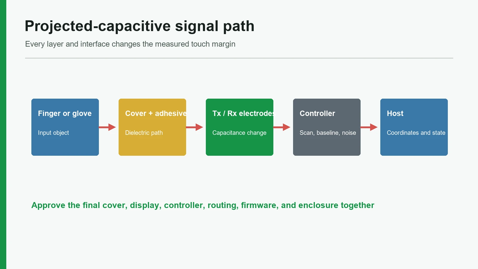
From electrode changes to coordinate output
A projected capacitive sensor does not directly produce screen pixels. It produces measurements distributed across electrodes or nodes. The controller turns that analog pattern into contacts through a sequence such as the following:
- Excite and acquire. TX lines are driven and RX responses are converted, or individual self-capacitance electrodes are measured.
- Normalize. Raw measurements are compared with no-touch baselines and compensated for drift.
- Detect. Candidate regions must exceed controller-defined signal and consistency criteria.
- Interpolate. Signal ratios on adjacent electrodes estimate a position between physical electrode centers.
- Filter. Temporal and spatial filters reduce jitter and interference, with a latency and responsiveness tradeoff.
- Track. Contacts receive identities so motion can be followed across frames.
- Report. Processed contact status and X/Y values are sent to the host.
Physical electrode pitch is coarse spatial sampling, not the same as reported coordinate resolution or absolute accuracy. Microchip's example shows interpolation between neighboring electrode amplitudes and also explains that longer measurements may improve resolution while reducing responsiveness. A specification that says “4096 × 4096 resolution” but omits edge error, linearity, jitter, finger size, report rate, display registration, and test fixture tells an integrator very little.
The host contract should be explicit. For Windows HID touch devices, Microsoft identifies contact ID, X/Y coordinates, tip state, and contact count among the touchscreen report elements. USB-IF's HID Usage Tables 1.7 assigns the Touch Screen usage to the Digitizers page. Linux's current multi-touch protocol uses Type B slots and tracking IDs for identifiable contacts. An embedded controller may use none of these, but it still needs an equivalent definition: byte order, coordinate origin, orientation, valid range, contact lifecycle, error handling, power states, and firmware-version control.
Projected capacitive sensor materials and constructions
There is no single canonical film stack. The correct construction depends on transparency, display size, resistance, border width, optical criteria, tooling, bend requirements, controller channels, and environmental exposure.
| Construction choice | Function | Engineering benefit | Design cost or limit |
|---|---|---|---|
| ITO on glass or film | Transparent TX/RX electrodes | Established optical sensor construction | Sheet resistance, pattern visibility, routing border, and bend limits must be managed |
| Copper on PCB or flex | Opaque capacitive electrode | Familiar circuit fabrication and low conductor resistance | Unsuitable across a transparent viewing area |
| Two-layer orthogonal grid | TX and RX on separate insulated layers | Straightforward row/column crossings | Extra interfaces, thickness, alignment, and optical effects |
| Single-layer diamond grid with bridges | Rows and columns share one sensor surface; insulated bridges complete one axis | Can reduce sensor-layer count | Bridge resistance, isolation, visibility, yield, and border routing need control |
| Rear shield or ground structure | Reduces coupling from the display or rear environment | Can improve noise control in the intended direction | Added capacitance can reduce sensitivity if geometry is poorly chosen |
| Full optical bond | Couples cover, sensor, and display without a designed air gap | Can improve optical/mechanical integration | Rework, stress, adhesive cure, bubbles, and material compatibility become process risks |
Infineon's single-layer example uses diamond electrodes with a 5–10 mm pitch and narrow bridge/gap features. That range belongs to the illustrated design, not every screen size or controller. The same paper shows the central tradeoff: larger pitch can recover touch coupling through a thicker cover, yet can increase positional nonlinearity between electrodes. Electrode geometry and cover thickness must be selected together.
Adhesive is an electrical material as well as a bond. Air bubbles or trapped moisture change the field because the front panel, PCB, and adhesive form part of the dielectric system. A production drawing should specify bond area, adhesive family, nominal thickness, void criteria, cure/lamination process, edge seal where needed, and the surfaces to which optical or mechanical criteria apply.
Integration limits, failure chains, and when PCAP is not best
Most PCAP failures are system interactions. The panel can pass incoming inspection and fail after bonding to the production display, after a cable reroute, after a grounding change, or only when a wet glove touches the bezel. The correct response is not to request “more sensitivity” without identifying the signal path.
| Design condition | Electrical or mechanical effect | Observable symptom | Verification response |
|---|---|---|---|
| Thicker cover lens or air gap | Weaker finger-to-electrode coupling | Missed light touches; poor response between electrodes | Test the actual lens, adhesive, finger target and controller tuning across the active area |
| Thick or loose insulating glove | Smaller and more variable touch signal | Intermittent contact, higher force, edge dropout | Define glove material, thickness, fit, humidity and user action as test inputs |
| Conductive droplets or a water film | Broad capacitance shift across nearby nodes | False contacts, blocked touch, contact merging | Separate dry, droplets, runoff, wet-finger and post-wet recovery criteria |
| LCD switching or backlight coupling | Periodic common-mode/differential noise | Jitter, false touches or missed contacts | Test production display patterns, brightness states, power modes and cable routing |
| Weak or shifting ground reference | Reduced return-path stability | Behavior changes by charger, enclosure or user grounding | Verify controller, chassis, display backplate and cable ground paths in the final assembly |
| Parallel high-speed cables near FPC | Capacitive/inductive interference | Localized noise or mode-dependent errors | Freeze routing/shielding before final tuning; retest after harness changes |
| Bond stress, support error or thermal mismatch | Gap change, bubbles, adhesive migration or delamination | Drift, cosmetic defects, local dead zones | Test bonded assemblies through thermal and mechanical loads, then recheck coordinates |
| Filtering set too aggressively | Signal smoothing and delayed state changes | Stable coordinates but sluggish gestures or release | Measure latency, report cadence, jitter and release behavior together |
Display switching is a major internal noise source. Inadequate immunity causes jitter, false touch, and missed touch, while changes to cable routing or shielding can require sensor retuning. Keep sensitive RX paths away from switching signals and cross unavoidable TX/RX paths at right angles. These are design-review principles; the selected controller's current hardware guide remains the controlling layout document.
Water tolerance requires equally precise language. Conductive liquid changes capacitance. A controller may classify droplets or suppress broad water signatures, but a spill-tolerant interface is not necessarily operable while submerged. Infineon explicitly distinguishes tolerated splashes from total immersion. IEC 60529 classifies protection provided by the finished enclosure, so neither a cover lens nor a touch sensor alone proves an IP rating.
A PCAP construction is not the best choice when the required input object is arbitrary and nonconductive, continuous submerged operation is mandatory, or a safety action requires deterministic physical travel and tactile state independent of software. It may also be the wrong choice when the product cannot allocate time for display-level EMC tuning, glove definition, bonding trials, and finished-assembly testing. A sealed membrane switch versus capacitive touch comparison can expose those requirements before industrial design locks the front panel.
Project inputs needed before sensor design
A useful PCAP request package describes one assembled device and its operating conditions. Sending only a display diagonal, outer glass size, and desired interface shifts unresolved risk to later prototypes.
Mechanical and optical inputs
- Dimensioned cover-lens drawing: material, thickness, edge treatment, holes, curvature, border print, viewing area, active area, tail exit, coatings, and cosmetic zones
- Lens-to-sensor and sensor-to-display bond method, adhesive family and nominal thickness
- Display maker and exact module number, polarizer surface, active area, bezel, backplate, mounting points, and permitted gap
- Enclosure metalwork, gasket, grounding features, nearby fasteners, bezel height, drainage path, and expected assembly loads
- Optical targets and test methods for luminance, reflection, haze, color shift, pattern visibility, bubbles, particles, Newton rings, and display registration
Electrical and host inputs
- Candidate controller and approved panel-size/channel range, or permission to propose a controller-panel pair
- Supply rails and tolerance, interface voltage, communication protocol, connector, FPC length, bend zones, interrupt/reset lines, firmware update path, and ESD protection concept
- Display interfaces, pixel clock, refresh modes, backlight topology, PWM range, chargers, motors, radios, high-speed harnesses, and their physical routes
- Required contacts, coordinate range, orientation, report rate, latency, edge behavior, gesture ownership, wake behavior, diagnostics, and firmware revision control
Use-condition inputs
- Bare finger size/action and any stylus model
- Every required glove by material, construction and thickness—not “works with gloves”
- Dry, condensation, droplets, flowing water, wet finger, cleaning liquid, salt contamination, or post-wet recovery states
- Temperature and humidity profiles, sunlight, contamination, cleaning chemicals, vibration, impact, expected service handling, and false-touch consequences
When the display, bonding, controller board, enclosure and host are supplied as one design responsibility, a capacitive touch HMI assembly can reduce interface gaps. It does not remove validation. It makes ownership of the complete stack easier to define. The custom capacitive touch panel design guide can be used to turn these inputs into a drawing and sample-approval package.
Verification matrix: test the stack, not an isolated panel
A PCAP qualification plan should name the assembly revision, controller firmware, display mode, power source, enclosure ground state, finger or glove, surface condition, environment, test method, observable output, and acceptance criteria. “Touch works” is not reproducible.
| Test block | Representative conditions to define | Observables | Acceptance owner / reference |
|---|---|---|---|
| Baseline functional map | Bare finger, center/edge/corner, single/multiple contacts, all display patterns and brightness states | Missed/false contacts, linearity, jitter, latency, report rate, edge error | Product specification; controller diagnostic method |
| Glove and stylus | Exact part/material, thickness, fit, dry/wet state, temperature, touch motion | Detection force/behavior, drag continuity, release, unintended contacts | Product use case; no generic “glove mode” pass |
| Moisture and cleaning | Droplets, film, runoff, wet finger, cleaner residue, recovery time | False contacts, touch suppression, recovery, permanent drift | Product requirement; enclosure/drainage design |
| ESD immunity | Accessible cover, bezel, connector and enclosure points; powered states | Reset, false touch, lost communication, data corruption, recovery | IEC 61000-4-2:2025 method with project-defined levels and criteria |
| Radiated/conducted RF | Operating modes, cables, ports, radios and display states | Jitter, false/missed touch, host faults, recovery | IEC 61000-4-3:2020 and IEC 61000-4-6:2023 methods; product-defined severity9 |
| Temperature change | Operating/non-operating profiles, dwell and transition rate | Baseline shift, touch map, bond defects, display registration | IEC 60068-2-14:2023 method plus product limits |
| Damp heat | Defined temperature, RH, duration, powered state and recovery | Drift, corrosion, optical defects, bond condition, touch behavior | IEC 60068-2-78:2025 method plus product limits |
| Mechanical assembly | Torque, bezel/gasket load, impact/vibration where applicable, cable strain | Local dead zones, coordinate shift, bubbles, delamination, connector faults | Finished-device mechanical plan |
| Host reporting | Boot, suspend/wake, contact add/move/remove, overflow, disconnect, firmware update | Contact IDs, X/Y range, stuck contacts, packet errors, recovery | Host protocol and system acceptance test |
IEC 61000 and IEC 60068 references are test methods, not evidence that a component is certified or that one severity fits every product. The product standard, regulatory plan, or OEM specification selects levels, orientations, durations, operating states, performance criteria, and sample counts. Finished medical or automotive equipment may have additional safety, EMC, software, usability, and regulatory obligations that a touch-panel supplier cannot approve on the device maker's behalf.
A touch-panel testing plan should preserve the controller firmware and physical routing used for the test. Tuning after qualification, changing the display, moving an FPC, changing adhesive thickness, altering chassis grounding, or replacing a charger can invalidate the relevant result. Golden samples and release records should bind the sensor drawing, controller hardware, firmware/configuration, display, bond stack, cable layout, and host build together.
Where PCAP fits well
A PCAP interface fits equipment that benefits from a cleanable glass surface, light touch, direct manipulation, and several tracked contacts. Typical contexts include industrial machine visualization, medical-device displays, vehicle center or auxiliary controls, marine displays, kiosks, laboratory instruments, and commercial equipment. The application name alone does not prove suitability.
For an industrial HMI, display noise, protective gloves, grounding and false activation may dominate. For a medical device, cleanability and usability matter, but finished-device risk management and regulatory validation remain with the legal manufacturer. In a vehicle or marine display, temperature, sunlight, water, conducted/radiated disturbances and user bracing can alter touch behavior. Kiosks may prioritize impact-resistant cover glass and edge accuracy. Each case changes the stack and test matrix, not the underlying definition of PCAP.
Frequently asked questions
What is projected capacitive touch panel technology?
Projected capacitive touch panel technology uses conductive electrodes behind an insulating cover to sense local capacitance changes. A controller scans the electrodes, compares measurements with an untouched baseline, identifies contact regions, interpolates X/Y positions, and reports those contacts to a host. The display beneath the sensor is a separate subsystem.
What is the difference between a PCAP touch panel and a capacitive touch sensor?
A projected capacitive sensor is the patterned electrode element. A PCAP touch panel usually includes that sensor plus a cover lens, adhesive, FPC, and sometimes a controller. A complete touch display adds the LCD or OLED, bonding, controller electronics, enclosure interfaces, firmware, and host reporting.
Why does mutual capacitance support multi-touch better than basic self capacitance?
Mutual capacitance measures each TX/RX intersection as a node, so multiple signal peaks can be associated with distinct X/Y positions. A basic self-capacitance row/column scan identifies active rows and columns but can produce ambiguous intersections when several contacts occur at once. Some controllers combine both methods.
Does thicker cover glass always stop a projected capacitive sensor from working?
No. Thicker glass weakens finger-to-electrode coupling, but electrode pitch, sensor pattern, material permittivity, adhesive, controller noise performance, tuning, glove conditions, and grounding also matter. The actual cover, sensor, display, controller, and enclosure must be tested together; a generic maximum thickness is not transferable across designs.
Can a PCAP touchscreen work with gloves?
It can work with defined gloves when the stack and controller preserve enough signal margin. Glove material, thickness, fit, compression, humidity, cover thickness, electrode pitch, noise, and touch action all affect detection. “Glove compatible” should name the exact glove and test conditions instead of acting as a blanket specification.
Is a water-tolerant PCAP panel waterproof?
No. Water tolerance describes specified behavior with conditions such as droplets, splashes, runoff, or a wet finger. Conductive liquid changes the sensor field, and normal operation during submersion is a different requirement. IEC 60529 also rates the finished enclosure, not a loose touch sensor or cover lens.
What does the touch controller send to the host?
A controller normally sends processed contact data such as contact identity or state and X/Y coordinates, often through a serial bus, USB, or a product-specific link. The exact report format, coordinate range, orientation, timing, contact lifecycle, diagnostics, and power-state behavior must be defined for the host integration.
Which tests should be run before approving a PCAP stack?
At minimum, map touch behavior across the active area and edges, then test the actual display modes, gloves or stylus, moisture states, grounding, power sources, cables, ESD, RF immunity, temperature/humidity conditions, mechanical loads, and host reporting. Use applicable standards as methods, with product-specific severities and pass criteria.
Review the PCAP stack before freezing the device
The useful design review is not “glass thickness plus screen size.” It aligns the cover, adhesive, electrode pattern, display, controller, FPC, grounding, enclosure, firmware, host protocol, operating objects, contamination states, and acceptance matrix. JASPER can be considered as one source for reviewing and producing that stack through its PCAP panel and HMI-assembly routes; suitability still depends on documented project inputs and finished-device verification.
Technical References
- Source: Infineon Industrial Capacitive Touchscreen Design Made Simpler. Accessed 2026.
- Source: Microchip TB3064 Projected Capacitive Touch Sensing Theory. Accessed 2026.
- Source: Microchip AN2934 Capacitive Touch Sensor Design Guide. Accessed 2026.
- Source: STMicroelectronics AN4313 Projected Sensor Design Guidelines. Accessed 2026.
- Source: Microsoft Required HID Top-Level Collections for Touchscreen. Accessed 2026.
- Source: USB-IF HID Usage Tables 1.7. Accessed 2026.
- Source: Linux Kernel Multi-touch Protocol Documentation. Accessed 2026.
- Source: IEC 60529 Degrees of Protection Provided by Enclosures. Accessed 2026.
- Source: IEC 61000-4-2:2025 Electrostatic Discharge Immunity. Accessed 2026.
- Source: IEC 61000-4-3:2020 Radiated RF Immunity. Accessed 2026.
- Source: IEC 61000-4-6:2023 Conducted RF Immunity. Accessed 2026.
- Source: IEC 60068-2-14:2023 Change of Temperature. Accessed 2026.
- Source: IEC 60068-2-78:2025 Damp Heat Testing. Accessed 2026.
Review the complete capacitive touch stack before release
Send the cover, artwork, active area, display, electrode, controller, tail, environment, and acceptance states for an engineering review.