
A custom capacitive touch panel is a controlled system of cover geometry, sensor pattern, dielectric stack, FPC, controller, display, enclosure, firmware, and validation evidence. Release those interfaces together.
JASPER certifications: ISO 9001, ISO 13485, IATF 16949, and ISO 14001.
1. Start With the Installed PCAP System, Not the Cover Artwork
A projected-capacitive panel is a signal chain. The user couples through a dielectric cover into an electrode matrix or discrete sensor; an FPC carries low-level signals or a processed digital interface; a controller measures and classifies the event; host software decides what the equipment does. The display, charger, metal bezel, ground, bonding stack, liquid, glove, and enclosure can change that chain.
Finger / approved glove / water or cleaning contact
v
Surface coating + cover lens + decorative ink border
v
Bond layer or intentional gap + PCAP sensor electrodes
v
FPC tail + connector + ground / shield strategy
v
Touch controller + configuration + firmware revision
v
Display / power / enclosure / host logic + operator feedback
Microchip’s 74-page QTAN0080 maXTouch Sensor Design Guide treats electrode pattern, pitch, substrate, front panel, shielding, and tail routing as connected decisions. Infineon’s industrial capacitive touchscreen paper adds controller choice, signal-to-noise ratio, display noise, and industrial stack integration. Those sources explain why an attractive cover drawing cannot approve the installed interface.
The purchased scope must also be explicit. JASPER’s custom capacitive touch panels may be considered when an OEM needs a custom physical front, sensor, FPC, adhesive, gasket, lighting, or assembly review. The quotation still has to state whether JASPER, the controller vendor, another integrator, or the OEM owns electrode design, controller selection, tuning, firmware, display bonding, enclosure sealing, and final-equipment validation.
Coordinate PCAP over a display is not the only architecture. Discrete capacitive keys, sliders, and wheels can sit behind an opaque printed cover and use PCB or FPC electrodes. A cover-lens-only purchase is different again. The controlled drawing and quotation should name which of these is actually being supplied.
2. The Ten Design Gates for Custom Capacitive Touch Panel Design
The ten gates below convert capacitive touch panel design into auditable decisions. A supplier should be able to show the named drawing, configuration, or test record—not merely assert that an option is available.
| Gate | Acceptance evidence | Release blocker |
|---|---|---|
| 1. Scope and ownership | Cover, sensor, controller, firmware, display, bond, seal, and validation owners appear in the quote and drawings | “Touch panel included” with no responsibility boundary |
| 2. Geometry and datums | One origin controls cover, view area, touch area, targets, mask, bond, bezel, and tail | “Active area” means different things in different files |
| 3. Sensor/controller pairing | Controller family, matrix/channel map, electrode source, tuning access, and edge behavior are reviewed together | Electrode artwork is frozen before controller and stack |
| 4. Cover lens and ink | Substrate, thickness, coating, print stack, border, aperture, dead front, and inspection are controlled | Cover is specified only as “glass” or “plastic” |
| 5. Dielectric stack and bond | Every coating, ink, adhesive, gap, sensor, and support layer has a nominal, tolerance, and owner | Ink steps, bubbles, air gaps, or substitutions are unmanaged |
| 6. FPC and controller location | Pinout, contact side, bend zone, mating part, raw/digital boundary, ground, shield, and strain relief agree | Tail route is added after the sensor is complete |
| 7. Display and noise | Installed conductor/noise map and worst powered states are in the validation plan | Only an isolated bench sample is tuned |
| 8. Water, glove, and feedback | Named inputs and liquids have accepted, rejected, locked, fault, and recovery states | “Works wet” is one unchecked requirement |
| 9. Bezel, seal, and enclosure | The test boundary includes the housing, bond/gasket, openings, fasteners, and tail exit | A flush face is called waterproof |
| 10. Approval and change control | Sample IDs, revisions, evidence, variation, deviations, and substitutions are controlled | One visually good sample becomes the golden unit |
Gate 1 — Define the supplied assembly and engineering owners
Start by writing the assembly boundary in nouns. Is the purchase a printed cover lens, cover-plus-sensor, sensor-and-controller module, display-bonded assembly, or complete HMI front? Which party creates the electrode pattern? Who selects and programs the controller? Who owns tuning, production configuration, diagnostics, host mapping, enclosure ingress testing, and the applicable equipment standard?
A good responsibility matrix uses the same wording in the request for quotation, supplier proposal, drawing notes, bill of materials, firmware record, and validation plan. A mismatch is a release stop. If a supplier quotes “complete touch solution” but excludes host behavior and installed-equipment testing, the drawing should say so without euphemism.
Evaluate each integrator against the exact supplied assembly, controller boundary, display-bonding scope, tuning ownership, validation evidence, change control, and lifecycle support. No manufacturer name removes the need to define ownership.
Gate 2 — Separate outside, view, active, target, mask, and bezel geometry
A PCAP panel drawing needs more than an overall outline. At least six geometries can overlap:
- cover-lens outside dimension;
- display view area and display active area;
- touch active or guaranteed sensing area;
- user target area for each icon, slider, or gesture;
- clear aperture and decorative ink or black-mask border;
- enclosure opening, bezel overlap, adhesive border, and sensor routing margin.
The panel drawing must distinguish outside dimension, display viewing area, touch active area, user key area, bezel opening, and FPC geometry. Define every term in the drawing legend; reusing AA for both display and touch active areas invites a registration error.
Choose one primary datum and coordinate origin. Dimension the display, sensor, icon centers, cover printing, adhesive, housing opening, and tail exit from that system. Also specify display orientation and X/Y direction. A sensor file mirrored relative to the cover can still be internally correct; the common assembly drawing catches the system error.
the supplier overlays all released layers at 1:1 scale and reports registration to the common datums.
mechanical CAD uses the cover center, artwork uses a trim edge, and controller mapping uses an unmarked sensor corner.
Gate 3 — Pair the electrode pattern with the controller and cover stack
The visible icon is not the electrode specification. Coordinate PCAP commonly uses intersecting transmit and receive structures; discrete buttons may use self-capacitance or mutual-capacitance geometries. Electrode pitch, gap, border behavior, routing, parasitic loading, and controller acquisition method interact.
Microchip QTAN0080 documents several maXTouch pattern families and treats the front-panel and sensor construction as pattern inputs. Texas Instruments’ CapTIvate Design Guide likewise connects overlay, electrode geometry, routing, ground, noise, moisture, and tuning. These are controller-family guides—not permission to copy one diamond, button diameter, or shield into another design.
Freeze these items together:
- Controller device or approved family;
- Sensor architecture and electrode source file;
- Matrix or channel mapping;
- Cover/print/bond/sensor stack revision;
- Edge and corner behavior;
- Controller configuration and firmware revision;
- Raw-data or diagnostic access needed for validation;
- Change-approval owner.
the sensor design review names the controller documentation revision and the production-intent cover stack.
a generic PCAP sensor is ordered first and “firmware tuning” is expected to compensate for every mechanical and noise condition later.
Gate 4 — Treat touch sensor cover lens design as electrical geometry
Touch sensor cover lens design includes the substrate, nominal thickness and tolerance, coating, curvature/flatness, edge treatment, print system, window, dead-front ink, metallic decoration, adhesive interface, and production variation. Microchip AN2934 documents the directional relationship: increasing the dielectric distance reduces touch coupling and changes the electrode/sensitivity design required. It does not establish one maximum glass or plastic thickness for all controllers.
| Cover route | Useful starting condition | Design review before release |
|---|---|---|
| Strengthened glass | Rigid optical front, hard surface, second-surface print | Edge/holes, strength target, ink, coating, flatness, bond stress, optical stack |
| PMMA / acrylic | Machined or printed transparent plastic lens | Scratch protection, chemical list, thermal/UV exposure, flatness, bond compatibility |
| Polycarbonate | Impact-oriented plastic front or shaped geometry | Hardcoat, chemical stress cracking, optical requirement, print and dimensional stability |
| Printed film over support | Thin decorated face with separate structural backing | Support flatness, adhesive, edge seal, window clarity, liner and assembly handling |
The ink border is functional. A thick black mask creates a step for the optical or structural adhesive. A conductive metallic ink can alter the field. A dead-front icon changes the local optical stack. Put print order, cured thickness profile where critical, registration tolerance, conductive-material restrictions, and lit/unlit inspection conditions on the artwork package.
a supplier receives native artwork plus a controlled PDF, color references, layer order, window transmission requirements, and the exact sensor relationship.
a last-minute decorative ink substitution is approved by appearance alone.
Gate 5 — Control the full dielectric stack and bonding process
The capacitive stack is every layer between the operator and the electrodes—not just the cover substrate.
Operator contact
surface finish / anti-glare / anti-fingerprint treatment
cover lens
decorative ink, black mask, dead-front or logo layers
OCA, LOCA, pressure-sensitive adhesive, filler, or intentional gap
transparent or opaque sensor substrate and electrodes
optional shield / display gap / display module
mechanical support and enclosure
Texas Instruments identifies labels, inks, adhesives, transition materials, and air gaps as mechanical/electrical inputs. An uncontrolled air pocket changes the dielectric path and can vary across the panel. An intentional display air gap may be valid; an accidental sensor-to-cover void is a process defect unless the approved design says otherwise.
Step coverage depends on adhesive stiffness and conformability. The CEF28XX/OCA 802XX family lists nominal options from 100 to 350 µm. That product-family range does not establish that a 350 µm film will fill a particular ink step or that JASPER runs that material.
bond drawings specify full/perimeter/local coverage, material code, nominal and tolerance, surface preparation, liner, assembly sequence, bubble/particle criteria, flatness, rework, and inspection.
“optically bonded” appears in the proposal with no adhesive, ink-step, process, or acceptance definition.
Gate 6 — Design the FPC tail, connector, and controller boundary together
Raw sensor traces are part of the analog sensing network. FPC length, trace adjacency, bends, connector, shielding, chassis proximity, and display cable can alter parasitic capacitance and coupled noise. Microchip’s MXTAN0208 PCB layout guide treats FPC routing, ground/guard/driven shield, stack-up, and bend regions as electrical design.
Two common ownership boundaries are:
Raw-sensor boundary:
electrodes → long/short FPC → connector → controller on OEM host PCB
Local-controller boundary:
electrodes → nearby controller/COF/COB → digital interface → OEM host
The first keeps active electronics off the panel but exposes raw sensor paths to the tail, connector, host layout, and installed noise. The second shortens sensitive paths but moves power, programming, firmware, diagnostics, interface, lifecycle, and change control onto the panel assembly.
A released tail drawing should show substrate and stack, conductor functions, pin numbering, contact side, mating connector, stiffener, bend and keepout zones, one-time versus dynamic bend, shield and ground features, tail-exit seal, strain relief, test points, FPC location, and fold information.
the controller boundary and mating PCB appear in the same interface control document.
an enclosure change folds the FPC across a noisy cable or sharp housing edge after touch tuning is complete.
Gate 7 — Map the display, ground, shield, metal, and noise sources
A sensor that passes on an isolated bench has not passed inside the product. Mark these items on one installed-system drawing:
- LCD/OLED outline, touch-to-display gap, display FPC, and driver electronics;
- switch-mode regulators, chargers, LED/backlight drivers, motors, relays, heaters, radios, and antennas;
- metal bezel, chassis, fasteners, decorative metal, and conductive coatings;
- sensor, raw traces, controller, ground, guard, driven shield, and cable shields;
- ESD-accessible edges, seams, connectors, and tail exits;
- power, display-refresh, radio, charging, sleep, startup, and fault modes.
Infineon identifies display-generated noise, cover construction, controller SNR, grounding, and shielding as linked industrial-PCAP variables. The useful design artifact is a conductor/noise map with each item labeled as aggressor, victim, reference, or barrier. “Add ground everywhere” is not a method; nearby ground can reduce coupling or reshape the field.
IEC 61000-4-2:2025 is the current third-edition ESD immunity test method for electrical/electronic equipment. It specifies test levels, waveform, setup, procedure, calibration, and uncertainty. The applicable product standard and risk plan still choose the test levels and acceptance criteria. A loose sensor or continuity test is not an IEC 61000-4-2 equipment pass.
touch raw data and host events are observed through the worst approved power/display/noise states in the production enclosure.
tuning is frozen before the display, charger, metal, and production cables exist.
Gate 8 — Specify water, glove, cleaning, and feedback as states
Works with gloves omits the glove material, thickness, fit, wetness, wear, temperature, touch object, target, and controller mode. Works wet omits droplets versus film, runoff versus pooling, conductive contamination, startup state, wipe behavior, lockout, recovery, and false-touch acceptance.
Create a state table before tuning:
| Input / condition | Required response | Evidence to retain |
|---|---|---|
| Approved bare finger, dry | Accept valid targets; reject excluded zones | Raw/processed data, host event, sample and revision |
| Named dry glove | Accept specified targets and gestures | Glove ID/condition, cover stack, controller configuration |
| Named wet or contaminated glove | Project-specific accept, reject, or lock state | Liquid/soil definition, repetitions, recovery record |
| Droplets or thin film | No unsafe event; defined operation or lockout | Application method, orientation, duration, host log |
| Pooling at edge or bezel | Defined rejection, drainage, lockout, or fault | Enclosure state, location, volume/method, recovery |
| Cleaning wipe / disinfectant | Defined cleaning mode and post-wipe recovery | Chemical, wipe material, cycles, dwell and inspection |
| Sleeve, palm, tool, unintended region | Reject or handle through named logic | Input object, coordinates, event log |
The controller can detect a signal; the host decides whether that signal becomes a command. ISO 9241-210:2019 covers human-centred design activities across the interactive-system lifecycle. For a PCAP HMI, sensor detection, disabled states, visible/audio/haptic feedback, and recovery should be approved together.
The water and glove tuning guide goes deeper into those states. The final URL is intentionally retained even if it is not yet live.
the requirement identifies what must be accepted, rejected, locked, reported, and recovered for each named condition.
sensitivity is increased until one thick glove works, without checking water, adjacent targets, display noise, or false events.
Gate 9 — Treat bonding, bezel, gasket, and tail exit as one enclosure boundary
A continuous glass face can simplify cleaning, but appearance does not establish ingress protection. Define the cover overlap, adhesive/gasket geometry, support surface, assembly compression, corners, holes, display window, housing seam, tail exit, connector path, fasteners, drainage, and service method.
IEC 60529 classifies degrees of protection provided by enclosures. Therefore, an IP claim must identify the exact enclosure and tested configuration. A cover lens, sensor, adhesive ring, or FPC subassembly cannot inherit an IP rating from a similar product or from a flat front surface.
Full optical bonding is also not automatically best. It may be selected for a controlled optical/mechanical stack, but it raises material, stress, rework, cleanliness, and process requirements. Perimeter bonding or an intentional display air gap may fit serviceable or cost-sensitive equipment, provided sensing, optics, sealing, and mechanical support are validated in that construction.
the drawing identifies which supplier-provided boundary is inspected and which OEM enclosure features complete the seal.
the RFQ requests IP67 touch panel but does not include the housing, tail exit, test orientation, or acceptance standard.
Gate 10 — Approve representative builds and freeze changes
A prototype answers only the question it was built to answer. A clear cover sample can approve print color yet say nothing about display noise. A hand-laminated sensor can demonstrate basic touch yet say little about production voids or bond stress. A tuned golden unit does not describe lot-to-lot variation.
Use staged prototyping:
- Sensor/stack coupon for coupling and controller feasibility;
- Production-intent cover, print, bond, sensor, tail, and connector;
- Installed powered equipment with production display, grounding, cables, enclosure, and host behavior;
- Multiple production-representative builds covering allowed material/process variation and the project’s environmental or lifecycle conditions.
JASPER’s prototyping process supports early fit and function planning. Confirm the PCAP controller, optical stack, bonding, noise, water and glove behavior, ESD, environmental limits, and life-test ownership in the project plan.
approval lists sample IDs, drawing/artwork/BOM revisions, controller and firmware/configuration revisions, display and enclosure, test states, results, deviations, and required changes.
procurement asks production to match an unlabeled sample kept in a desk drawer.
3. What a PCAP Panel Drawing Package Should Include
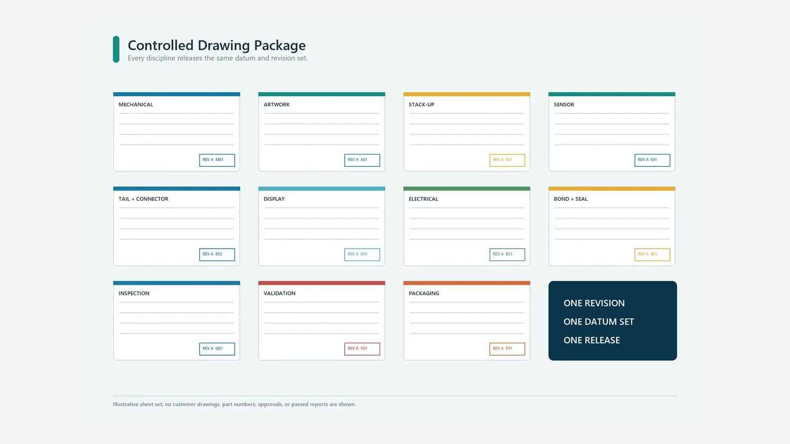
A PCAP panel drawing is a set of coordinated manufacturing and interface documents. Include 1:1 native CAD or vector files, controlled-view PDFs, construction and interface inputs, and clear revision relationships between every released file.
| File or sheet | Minimum controlled content |
|---|---|
| Cover mechanical drawing | Outline, thickness/tolerance, radii, holes, edge treatment, coating, flatness/curvature, datums, finish |
| Artwork and ink-border file | Native vector file, colors, layer order, windows, mask, dead front, metallic/conductive restrictions, registration, lit/unlit criteria |
| Geometry overlay | Cover OD, display VA/AA, touch active area, targets, sensor border, bezel, bond/gasket, housing opening, tail exit—all at one origin |
| Dielectric stack | Coating, cover, inks, adhesive/gap, sensor, shield, display, support, nominals/tolerances and material codes |
| Sensor pattern | Architecture, electrode artwork, pitch/gap where applicable, border, routing, orientation, controller/matrix map, keepouts |
| FPC and connector | Stack/conductors, outline, contact side, pinout, mating part, stiffener, bend/keepout, shield/ground, strain relief, test points |
| Controller/interface control | Device/family, power, raw-vs-digital boundary, I2C/SPI/USB or other interface, interrupt/reset, programming, diagnostics, configuration/firmware owner |
| Display/noise map | Display and cable, regulators, charger, LEDs, motors, radios, metal, chassis, ESD access, ground/shield connections |
| Bonding/sealing drawing | Adhesive/gasket code and geometry, surfaces, liner, assembly sequence, tail exit, cure/aging, inspection, rework boundary |
| Inspection plan | Critical dimensions, cosmetics, print/registration, continuity, pinout, lighting, bond defects, touch-function screen |
| Validation matrix | States, equipment mode, sample count, repetitions, environment, expected response, evidence, owner |
| Packaging/change control | Protective films, trays, FPC protection, labels, revision release, approved alternates and requalification triggers |
Manage functional tolerance chains
The worst permitted combination must still assemble, look correct, and retain the validated sensing geometry. Review chains rather than isolated dimensions:
Housing datum
opening / bezel / support variation
cover outline and print registration
bond or gasket location and thickness
sensor registration
display location and active image
FPC exit and connector route
= installed optical, mechanical, and sensing relationship
Typical chains include icon center to electrode center, display image to clear aperture, sensor border to metal bezel, adhesive edge to the view area, and FPC exit to the housing slot. Mark critical-to-function features and match tolerances to the actual process and inspection method. A tight number with no measurement method is decoration, not control.
Freeze digital ownership as carefully as hardware
Record controller configuration, tuning file, firmware binary/source ownership, programming fixture, version identifier, boot/reset behavior, host mapping, diagnostic interface, and update path. If the controller remains on the OEM PCB, the panel supplier still needs its electrical constraints before the sensor and FPC are released.
4. A Six-Step Design and Procurement Process
Step 1 — Submit the installed product inputs
Begin with the cover/enclosure CAD, display drawing, UI targets, operator and glove, cleaning/liquid conditions, intended sensor/controller boundary, FPC route, mating connector, metal/ground/noise environment, applicable equipment standards, and expected production context. A sketch can start a feasibility discussion; it cannot release registered artwork and electrodes.
If the architecture is not fixed, compare PCAP touch panels with the alternatives before committing. The related capacitive versus resistive guide owns that technology decision and is intentionally linked on its planned final route.
Step 2 — Freeze scope, datums, and architecture
Write the responsibility matrix. Select coordinate PCAP, discrete keys, slider/wheel, or cover-only scope. Set the common datum/origin, display and touch areas, UI rotation, controller location, host interface, and diagnostic requirement. At this stage, unresolved controller choice is a technical dependency, not a purchasing footnote.
A formal design review should produce an interface control drawing plus an open-issue list. Do not release cover tooling while the sensor border, ink mask, FPC exit, or display relationship remains initial.
Step 3 — Co-design cover, sensor, tail, and bond stack
Build the production-intent dielectric stack. Review cover material, thickness/tolerance, coating, print, ink-step profile, electrode pattern, sensor substrate, OCA/LOCA/PSA or intentional gap, FPC route, ground/shield, and support flatness in one meeting. Run device-specific rules from the chosen controller vendor rather than mixing dimensions from Microchip, Infineon, TI, and a generic supplier drawing.
The output is a revision-linked drawing set and bill of materials—not a collection of emailed screenshots.
Step 4 — Prototype the highest-risk interfaces first
If coupling through the proposed stack is uncertain, build a sensor coupon before decorated full-size glass. If optical bonding over a thick ink border is the highest risk, build a process coupon with the intended substrates and step. If display noise dominates, bring the production display, power tree, controller, ground, and FPC into the prototype early.
The best prototype order follows risk, not appearance. A beautiful sample can arrive after the controller, bond, or noise architecture has already failed.
Step 5 — Validate the installed powered assembly
Install the panel in the production-representative enclosure with display, cables, power, controller/configuration, host firmware, feedback, bezel, grounding, and seal. Exercise center, edge, corner, adjacent, held, rapid, invalid, startup, reset, sleep/wake, display, charging, radio/noise, named gloves, liquid/cleaning, and recovery states as applicable.
For ESD, ingress, environmental, medical, automotive, marine, or other regulated equipment, the applicable finished-equipment standards and risk plan decide the method, levels, sample count, and pass criteria. Component manufacture does not equal finished-device approval.
Step 6 — Approve evidence and lock production changes
Approve sample IDs against the exact drawing, artwork, BOM, controller, firmware/configuration, display, enclosure, assembly process, and test matrix. Record deviations and corrective actions. Then identify requalification triggers: cover or ink supplier, coating, adhesive, sensor substrate, electrode artwork, FPC stack, connector, controller, firmware, display, housing, gasket, ground, or process changes.
The goal is not a frozen product forever. It is a controlled decision about which changes require review, sample approval, partial retest, or full system revalidation.
5. Validation Matrix and Failure Chains
Validation and sample-approval matrix
| Area | Representative condition | Evidence required before approval |
|---|---|---|
| Geometry and fit | Cover, windows, sensor, FPC, connector, housing | Measured values tied to sample IDs and drawing revision |
| Printing and optics | Lit/unlit mask, color, dead front, window, defects | Approved master, inspection method, lighting/viewing condition |
| Bond and support | Ink step, bubbles, particles, flatness, stress, cure/aging | Process record, material lot, inspection and defined acceptance |
| Electrical interface | Continuity, pinout, supply, reset, communication | Fixture/program revision and recorded result |
| Touch function | Center, edge, corner, adjacent, hold, rapid sequence | Raw/processed data, host event and accepted behavior |
| Invalid input | Palm, sleeve, tool, wet region, excluded area | Rejected/locked/fault response and event log |
| Display and noise | Refresh modes, brightness, charging, radio, motors, LEDs | Worst-state observations in production-representative stack |
| Startup and recovery | Power cycle, brownout, reset, wet startup, disconnect | Defined safe state, recalibration rule and recovery evidence |
| Enclosure boundary | Adhesive/gasket, seam, tail exit, connector path | Test record for the exact named assembly boundary |
| Production variation | Multiple covers, sensors, bonds, controllers and assemblies | Distribution versus approved limits and disposition |
| Documentation | CAD, artwork, BOM, firmware, configuration, test plan | One matching released revision set |
Failure chain: omission to field symptom
| Omitted control | Physical or system mechanism | Likely symptom | Evidence that closes the chain |
|---|---|---|---|
| Common datum | Cover, display, sensor, and bezel stack independently | Offset target, clipped image, weak edge | 1:1 layer overlay and measured registration |
| Complete dielectric stack | Ink, adhesive, gap, or liner changes coupling | Sensitivity spread or local dead/false regions | Cross-section/stack record plus raw-data distribution |
| Controller-pattern review | Matrix/pitch/loading does not fit controller | Poor tracking, edge error, tuning dead end | Device-specific design review and production configuration |
| FPC/noise map | Raw traces couple to display, charger, metal, or cable | Mode-dependent false or missed touch | Installed worst-state noise log and revised routing/shield |
| Named water/glove states | Threshold change solves one input but harms another | False events, lockup, slow recovery | State matrix with accepted/rejected/recovery results |
| Bond-process window | Ink step, particles, flatness, or cure varies | Bubbles, stress, delamination, optical or touch variation | Material/process lot record and inspection criteria |
| Enclosure test boundary | Cover face is mistaken for sealed equipment | Ingress at edge, tail exit, seam, or connector | IEC 60529-based equipment test for exact boundary, if required |
| Revision freeze | Material or firmware changes without review | Production drift from approved sample | Change notice, impact assessment, requalification record |
A source ledger cannot replace test evidence, but it prevents universal claims from entering the plan. Microchip, Infineon, TI, 3M, IEC, and ISO define dependencies and methods. The OEM and its suppliers must still produce results for the actual stack.
6. When a Custom PCAP Panel Is Not the Best Choice
A custom PCAP construction is not automatically the best interface.
Choose a standard off-the-shelf touch/display module when its outline, view/active area, controller, interface, cover, operating conditions, availability, and lifecycle fit the product. Customizing only the bezel artwork around a proven module may reduce engineering and supply risk.
Choose a tactile membrane switch or physical control when deliberate force, physical confirmation, eyes-free location, simple contact closure, or a hardwired safety function outweighs a flush dynamic surface. A capacitive key has no inherent travel or snap.
Choose resistive touch when the approved input object and interaction require pressure-based operation and the optical, gesture, wear, and integration tradeoffs are acceptable. The technology decision belongs before a custom PCAP drawing is released.
Use a mechanical emergency stop, guarded switch, redundant control, or other risk-assessed architecture when a touch surface alone cannot meet the safety function. For medical devices, automotive systems, marine equipment, or machinery, component manufacturing is only one input to finished-equipment validation and regulatory approval.
Full optical bonding may also be the wrong construction when serviceability, low-volume rework, stress, material compatibility, cleanliness, or process ownership cannot be controlled. An intentional air gap or perimeter bond can be legitimate if the resulting optics, touch behavior, mechanics, and enclosure meet the defined requirement.
7. Stop Conditions Before Tooling or Production Release
Stop the release if any item remains unresolved:
- The supplied assembly and controller/firmware/tuning ownership are not written.
- Display view area, touch active area, user target, mask opening, and bezel geometry are mixed.
- Sensor pattern, controller family, and production-intent cover stack have not been reviewed together.
- Cover substrate, coating, ink stack, conductive-decoration restrictions, adhesive/gap, and sensor are not one controlled stack.
- FPC pinout, contact side, bend, mating connector, ground/shield, and controller boundary are incomplete.
- The production display, power, metal, cables, and noise modes are absent from validation.
- Glove, water, cleaning, invalid-input, feedback, lockout, and recovery states are vague.
- An IP or ESD result is requested without the exact equipment boundary, standard, setup, level, and acceptance criteria.
- Prototype samples do not represent the approved production materials and process.
- Sample approval lacks IDs, matching revisions, conditions, evidence, deviations, or disposition.
- Material, controller, firmware, display, or process substitutions can occur without touch/optical/noise review.
- The release package contains unresolved requirements or editorial tokens.
8. Frequently Asked Questions
What should a custom PCAP panel drawing include?
A PCAP panel drawing package should include the cover mechanical drawing, artwork and ink border, common-datum geometry overlay, complete dielectric stack, sensor pattern, FPC/connector, controller interface, display/noise map, bonding/sealing details, inspection plan, validation matrix, and revision/change controls. Supply native CAD/vector files plus controlled PDFs.
When should the touch controller be selected?
Select the controller family before releasing the sensor pattern and FPC. The controller affects matrix or channel support, electrode design, loading, routing, shield strategy, tuning, diagnostics, host interface, firmware ownership, and test access. A future software team cannot reliably recover an incompatible physical stack.
How does cover-lens thickness affect capacitive touch?
Greater dielectric distance generally reduces finger-to-electrode coupling, so cover material, thickness, print, adhesive, gaps, electrode geometry, controller, ground, and noise must be designed together. Microchip AN2934 supports that relationship, but no single maximum glass or plastic thickness applies to every PCAP controller and input condition.
Is optical bonding required for every PCAP display?
No. Full optical bonding, perimeter bonding, sensor-to-cover lamination, and an intentional display air gap can each be valid. The choice changes optics, touch coupling, flatness, stress, sealing, cleanliness, process control, rework, and service. Validate the selected construction with the real cover, ink border, sensor, display, and enclosure.
Can a custom capacitive touch panel work with gloves and water?
It can when the named glove, liquid state, cover stack, sensor, controller/configuration, grounding, enclosure, host logic, and acceptance plan support the required response. Specify which inputs must be accepted, rejected, locked, reported, or recovered. ‘Works wet’ and ‘glove compatible’ are not complete engineering requirements.
Should the controller sit on the panel or the OEM main PCB?
Either boundary can work. A remote controller leaves raw sensor signals exposed to FPC length, connector, host layout, and noise. A local controller shortens sensitive paths but adds power, programming, firmware, diagnostics, communication, lifecycle, and change-control duties to the panel. Compare both before freezing the tail route.
Does a bonded glass front make the equipment IP65 or IP67?
No. IEC 60529 addresses protection provided by the enclosure. The tested configuration must include the relevant cover bond or gasket, housing, seams, holes, fasteners, tail exit, connector path, orientation, and acceptance target. A loose lens, sensor, or adhesive ring does not carry an enclosure IP rating by appearance.
What evidence should be approved before production?
Approve sample IDs against matching mechanical, artwork, stack, sensor, FPC, BOM, controller, firmware/configuration, display, enclosure, assembly-process, inspection, and validation revisions. Include geometry, optics, bond, electrical, touch, invalid-input, noise, startup/recovery, environmental, production-variation, and deviation records required by the project.
9. Submit the Panel Drawing or Display Outline
Send the cover and enclosure CAD, native artwork, display outline, touch targets, controller candidates or constraints, stack concept, FPC/connector, ground/noise map, glove/water/cleaning states, applicable equipment standards, and required approval evidence. A preliminary display outline is enough to start a boundary review; tooling needs the controlled package described above.
JASPER can be considered for an HMI assembly or physical panel review when its written project scope matches the requirement. The related the type of installed-system boundary that should be discussed; it is not proof of a universal result. Submit the files through the engineering review or request-a-quote route.
Technical References
- Source: Microchip QTAN0080 maXTouch Sensor Design Guide. Accessed 2026.
- Source: Microchip MXTAN0208 maXTouch Controller PCB Layout Guide. Accessed 2026.
- Source: Microchip AN2934 Capacitive Touch Sensor Design Guide. Accessed 2026.
- Source: Infineon Industrial Capacitive Touchscreen Design Guidance. Accessed 2026.
- Source: Texas Instruments CapTIvate Technology Guide. Accessed 2026.
- Source: 3M Optically Clear Adhesive Technical Data. Accessed 2026.
- Source: IEC 60529 Degrees of Protection Provided by Enclosures. Accessed 2026.
- Source: IEC 61000-4-2 Electrostatic Discharge Immunity. Accessed 2026.
- Source: ISO 9241-210 Human-Centred Design for Interactive Systems. Accessed 2026.
- Source: QTAN0080 maXTouch Sensor Design Guide. Accessed 2026.
- Source: industrial capacitive touchscreen paper. Accessed 2026.
- Source: CapTIvate Design Guide. Accessed 2026.
- Source: MXTAN0208 PCB layout guide. Accessed 2026.
- Source: 61000-4-2:2025. Accessed 2026.
- Source: 9241-210:2019. Accessed 2026.
- Source: 60529. Accessed 2026.
- Source: QTAN0080 maXTouch Sensor Design Guide (AN3908). Accessed 2026.
- Source: MXTAN0208 Design Guidelines for PCB Layouts for maXTouch Controllers. Accessed 2026.
- Source: AN2934 Capacitive Touch Sensor Design Guide. Accessed 2026.
- Source: Industrial Capacitive Touchscreen Design Made Simpler. Accessed 2026.
- Source: CapTIvate Technology Guide — Design Guide. Accessed 2026.
- Source: Optically Clear Adhesive Technical Resources. Accessed 2026.
- Source: CEF28XX/OCA 802XX Technical Data Sheet. Accessed 2026.
- Source: IEC 60529:1989+AMD1:1999+AMD2:2013 CSV, edition 2.2. Accessed 2026.
- Source: IEC 61000-4-2:2025, Electrostatic discharge immunity test. Accessed 2026.
- Source: ISO 9241-210:2019. Accessed 2026.
Release one coordinated PCAP drawing package
Send the cover and display CAD, artwork, sensor and FPC concept, controller boundary, bond stack, enclosure section, and validation plan.