
Silicone rubber keypad EMI shielding uses a conductive layer, filled elastomer, foil, mesh, or perimeter gasket to control electromagnetic coupling at the user-interface opening. It works only when the shield remains electrically continuous and has a defined bond to the equipment’s shield or chassis reference.
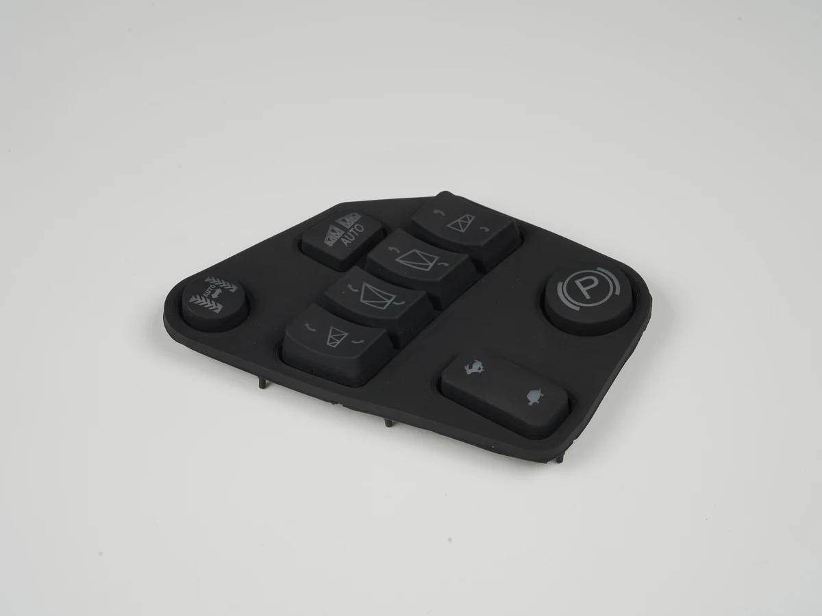
Silicone rubber keypad EMI shielding should be designed as part of the enclosure and PCB, not purchased as a coating option in isolation. For OEM silicone rubber keypads, the usual starting point is a separate conductive plane under the moving key geometry, bonded around the perimeter to a controlled chassis or shield reference. Conductive fillers, seam compression, openings for light, coating durability, and PCB return paths then determine the result. Carbon pills still serve as switch contacts; they do not form a continuous RF barrier. Final acceptance belongs at complete-equipment level because a material coupon cannot reproduce the keypad aperture, housing seam, cables, fasteners, or ground architecture.
Quick decision: choose the shield architecture before choosing the material
| Design condition | Practical starting architecture | Main benefit | Primary risk to verify |
|---|---|---|---|
| Broad keypad area, moderate travel, room for a separate layer | Printed conductive film or metalized foil below the keymat | Keeps the shield function outside most moving webs | Ground-tail impedance, creases, apertures, and assembly registration |
| Complex molded underside where a film will not seat | Silicone-compatible conductive coating on selected stationary surfaces | Conforms to three-dimensional geometry | Adhesion, flex cracking, thickness variation, abrasion, and masked keep-outs |
| Shield and environmental seal must share a molded component | Co-molded or bonded filler-loaded conductive silicone region | Integrates electrical contact and compliance | Higher hardness, force shift, molding control, and galvanic pairing |
| Leakage is concentrated at the bezel-to-housing seam | Perimeter conductive elastomer gasket plus a separate field shield | Closes a mechanical seam and can support sealing | Compression tolerance, flange flatness, fastener spacing, and corrosion |
| Display or illuminated window crosses the shield plane | Segmented metal mesh or transparent conductive window plus perimeter bond | Preserves visibility while continuing the shield | Window-to-frame bond, optical loss, mesh pattern, and edge discontinuities |
The table is a topology decision, not a promise of attenuation. Select the required frequency range, field exposure, product-level limits, and performance criteria before requesting a dB value from any material supplier.
Silicone rubber keypad EMI shielding is different from a conductive switch contact
A keypad assembly contains conductive parts with different jobs. A carbon pill or conductive contact coating bridges two PCB pads only while a key is pressed. An EMI shield must instead cover the coupling path with enough continuity to redirect field-induced current or ESD current without sending it through sensitive logic. A perimeter gasket maintains electrical contact across a housing seam. A molded silicone skirt or separate seal controls water and dust. One feature may contribute to two functions, but the drawing must name each function separately.
“Conductive silicone” does not describe the current-path geometry. Isolated contact pills leave most of the front-panel aperture unshielded. An underside coating can form a shield, but coating the moving web or bridging switch pads can alter feel or create unintended conduction. A perimeter ring closes a seam only when it also bonds to the field shield.
Use the Silicone Rubber Keypad Design Guide to establish the unshielded key geometry, force/travel curve, contact pattern, legends, and lighting first. Add the shield as a controlled layer with its own boundaries, bond points, and inspection characteristics.
A reliable architecture combines a field barrier, a perimeter bond, and a PCB return path
The shield stack should direct unwanted current around the keypad circuit and into the intended reference structure. The following reference architecture is not to scale and is not a universal grounding schematic:
USER / EXTERNAL FIELD / ESD
            ↓
┌──────────────────────────────────────────────┐
│ Legends + protective surface coating        │
├──────────────────────────────────────────────┤
│ Molded silicone keys, webs, skirt, light wells│
├──────────── stationary keep-out boundary ────┤
│ Conductive film / coating / mesh shield plane│──┐
├──────────────────────────────────────────────┤  │ short, wide bond
│ Insulating spacer or controlled air gap      │  │
├──────────────────────────────────────────────┤  ▼
│ Carbon pills over PCB switch pads            │  perimeter shield land
├──────────────────────────────────────────────┤  on PCB or metal frame
│ PCB: switch matrix + local protection        │──┐
│      continuous signal return plane          │  │ defined chassis/
└──────────────────────────────────────────────┘  └─shield reference
             HOUSING / BACKER / FASTENERS
The barrier may be a flexible film, a cured coating, a molded conductive region, or mesh. Its edge needs repeatable contact with a plated PCB land, conductive frame, or enclosure flange. That bond should be short and wide at RF, protected from paint and oxide where contact is required, and mechanically loaded without crushing the elastomer. The signal return plane still serves the switch matrix and controller. The shield reference may connect directly, capacitively, or at a controlled point depending on safety, isolation, cable, enclosure, and system architecture; the schematic and layout must show the chosen relationship.
Texas Instruments’ system-level ESD guidance explains why the return path matters: breaks in a plane force high-frequency current around a larger loop, increasing inductance and radiation. Its front-panel PCB design guidance also treats a keypad/display board as part of the shielded enclosure and distinguishes the shield structure from the controller return. Those principles support a keypad reference design, but the final node connection still requires product-specific EMC and safety review.
Conductive coatings, films, filled silicone, mesh, and gaskets solve different problems
No single shielding method wins every keypad program. A method should be selected against movement, land area, lighting, sealing, chemical exposure, rework, and the known coupling path.
| Method | Construction | Best fit | Key-feel effect | Lighting / legend effect | Manufacturing and validation concern |
|---|---|---|---|---|---|
| Printed conductive film | Silver or carbon pattern on a flexible carrier below the keymat | Flat or gently contoured field plane | Usually low if isolated from moving webs | Requires openings or transparent window treatment | Registration, crease control, trace neck-down, ground tail, laminate durability |
| Metalized foil | Aluminum- or copper-based flexible layer with a designed bond feature | High-conductivity plane with assembly room | Low when mechanically decoupled | Opaque; apertures must be controlled | Edge tearing, galvanic pairing, adhesive creep, bond impedance |
| Silicone-compatible coating | Flexible conductive coating applied to stationary underside areas | Three-dimensional molded geometry | Can rise or drift if coating enters flexure zones | Masking needed around light pipes and translucent legends | Surface preparation, cure, thickness, adhesion, abrasion, repeated flex |
| Filler-loaded conductive silicone | Carbon, nickel-graphite, silver-aluminum, or another qualified filler in silicone/fluorosilicone | Molded shield ring, ground pad, or integrated gasket | May increase local hardness and closure load | Usually opaque and can scatter light | Filler distribution, flash, bond to insulating silicone, resistivity, compression set |
| Conductive mesh | Metal mesh captured below the keypad or across a window | Rugged or optical areas where a solid opaque layer is unsuitable | Low if kept outside the web | Mesh can remain visible or reduce transmission | Edge termination, mesh distortion, corrosion, aperture pattern |
| Perimeter conductive gasket | Die-cut, molded, extruded, or form-in-place elastomer at the bezel seam | Closing a housing joint | None if separated from actuation geometry | Usually none | Compression tolerance, flange stiffness, fastener spacing, surface finish |
A printed film usually protects tactility because it remains outside the silicone web. A coating fits ribs or pockets that defeat a flat film. A filled-silicone ring accommodates tolerance and carries current, but it may not match the insulating keymat’s rebound or tear behavior.
One supplier example, ECP-SSE002, is a silver-filled silicone coating reported to adhere to silicone elastomers; its published values are 0.05 ohm surface resistivity, 100 micrometres dry film thickness, and 160°C maximum service temperature. These formulation-specific data are not finished-keypad results. WACKER’s ELASTOSIL R 573/50 A/B likewise demonstrates moldable conductive high-consistency silicone without claiming system attenuation.
Filler choice couples electrical and mechanical behavior. A peer-reviewed nickel-coated-graphite/silicone study compared 30%, 50%, and 70% filler by weight; increasing filler lowered resistivity and increased hardness in that formulation. The engineering implication is direct: the compound that improves current continuity may also change gasket load or tactile response. Test the chosen compound, not the filler name.
Grounding and gasket interfaces fail when the mechanical joint is treated as an ideal wire
A shield plane without a controlled bond can float or redirect current. Identify the land material and finish, contact area, compression, tolerance stack, clamp locations, and route to the shield reference. Conductive adhesive may aid assembly, but it should not become an undocumented compression-control feature.
TE Connectivity recommends 10%–20% compression for its cited grades and at least 2 mm material width or a width no smaller than thickness. Parker Chomerics gives a geometry-specific example: 5% minimum, 10% nominal, and 15% maximum height deflection for its rectangular/die-cut parts. These are supplier-specific rules. Put the selected grade, cross-section, and permitted deflection on the drawing.
Four interface details deserve a design review:
- Surface finish: paint, anodize, oxide, contamination, or adhesive can interrupt contact. Define exposed or plated lands and an inspection method.
- Compression control: use groove depth, stops, collars, or housing geometry. Include keymat, PCB, backer, and fastener tolerances.
- Galvanic compatibility: pair filler and flange for the humidity, salt, and chemical environment. Corrosion makes continuity temporary.
- Bond inductance: a long pigtail may pass a DC check yet fail at RF. Prefer a short, wide bond or distributed contacts.
Grounding does not replace input protection. Place protection near exposed signals and keep the discharge path away from the controller. Shielding also does not address tamper detection or trust boundaries; review those separately in HMI Hardware Security Boundaries for OEM Design.
PCB reference design should reserve shield lands before the keypad tooling is released
PCB and keymat drawings should share coordinates for switch pads, contacts, shield keep-outs, perimeter lands, LEDs, fasteners, and datums. Adding a shield land after routing often creates narrow necks or slots at the aperture edge.
Use a continuous return plane beneath the switch matrix where the architecture allows. Do not route matrix traces across plane breaks. Route LED drive with its return and keep power conversion away from key-scan nodes. For a cabled keypad PCB, define shield termination, signal returns, cable length, and filtering together; the cable may dominate emissions.
Use separate net names for shield and circuit return until the schematic defines their relationship. Add test points so a fixture can detect missing bonds, contamination, or film misregistration before final assembly.
Shielding can change key feel, legends, lighting, and sealing
Added layers change stack height or stiffness. Film can alter preload or wrinkle under short-travel keys; coating across a web may crack; filled silicone may be harder than the keymat. Freeze the force/travel target, then compare instrumented curves before and after conditioning.
Backlighting creates apertures. Keep opaque material out of light wells without opening an uncontrolled slot around each LED. Options include localized openings, film below the light guide, segmented mesh, or a transparent conductive display window. Check light leakage, brightness, color, and continuity on one sample.
Keep EMI coating on protected underside surfaces. Prevent overspray into contacts, translucent regions, or adhesive lands, and define masking datums plus cosmetic zones.
Environmental sealing remains an enclosure result. IEC 60529 classifies degrees of protection provided by enclosures; a loose silicone keymat or gasket cannot establish the assembled product’s IP rating. The shield and moisture seal may share a compressed perimeter, but both functions need their own acceptance criteria.
Common failure paths are discontinuities, uncontrolled compression, and the wrong test level
Shielding failures usually occur at interfaces rather than in the center of a material coupon.
| Failure path | What creates it | Observable symptom | Design or control response |
|---|---|---|---|
| Floating shield | Missing bond, insulated land, adhesive-only contact | Variable emissions/immunity by assembly or hand position | Define bond node, exposed finish, compression, and continuity test |
| Cracked coating | Coating crosses a high-strain web or has poor cure/adhesion | Resistance rises after actuation or thermal cycling | Mask flex zones; validate representative molded samples after conditioning |
| Aperture leakage | Oversized LED/display opening, split shield, narrow bridge | Failure only at certain frequencies or orientations | Reduce/segment aperture; bond window treatment to the perimeter plane |
| Crushed gasket | Tolerance stack or fastener torque exceeds grade limit | Permanent set, high closing force, loss after reassembly | Add hard stops and control groove depth, grade, torque, and flatness |
| Corroded joint | Incompatible filler/flange pair plus moisture or chemicals | Intermittent continuity after environmental exposure | Specify compatible materials, finish, edge sealing, and conditioned tests |
| PCB return detour | Matrix trace crosses plane slot; shield bond uses a long lead | ESD upset or radiated susceptibility despite a conductive layer | Restore local return path; shorten/widen bond; relocate protection |
| Coupon-to-system assumption | Material dB value accepted as equipment performance | Late chamber failure | Test material, subassembly, and complete equipment at separate gates |
Keypad shielding is the wrong primary fix when a cable, switch-mode loop, display interface, or connector dominates coupling. It is also a poor fit when the web cannot tolerate a conductive layer, no stable bond land exists, the filler/flange pair conflicts with the environment, or an optical opening dominates. A shield can, filtered cable, relocated circuit, or enclosure redesign may be more direct.
Verification must separate material data from keypad and complete-equipment evidence
Shielding effectiveness is test-method dependent. ASTM D4935-18(2026) covers planar material measurements under normal-incidence far-field conditions from 30 MHz to 1.5 GHz and excludes cables and connectors. SAE ARP6248 addresses conductive gasket materials and joint surfaces by stripline up to 40 GHz. Neither method reproduces a finished keypad enclosure. Use them to compare controlled specimens, then verify the assembly.
| Gate | Test article | Inputs held constant | Measurements / observations | Decision |
|---|---|---|---|---|
| Material qualification | Coating coupon, film, mesh, or conductive elastomer sample | Thickness, cure, filler/grade, substrate, frequency method, temperature | Resistivity or surface resistance; adhesion; hardness; supplier-method SE where relevant | Is the material stable enough to enter component trials? |
| Molded component | Representative keymat with production-intent geometry | Web thickness, coating mask, molded bond, post-cure, legends, light features | Force/travel curve; shield continuity; contact resistance; coating coverage; optical inspection | Does shielding preserve switching, feel, and manufacturability? |
| Keypad subassembly | Keymat, PCB, frame/backer, gasket, fasteners, cable | Torque, compression, land finish, bond topology, cable configuration | Bond resistance; key scan; light uniformity; pre-compliance emissions/immunity; ESD current-path behavior | Is the stack ready for equipment integration? |
| Environmental sequence | Production-intent subassembly before and after conditioning | Project-defined temperature, humidity, fluid, actuation, vibration, and reassembly sequences | Drift in force, resistance, adhesion, sealing, corrosion, and visual condition | Does the joint retain both electrical and mechanical functions? |
| Complete equipment | Final enclosure, firmware, cables, power supplies, accessories | Governing standard setup, operating modes, cable layout, performance criteria | Emissions, radiated/conducted immunity, ESD, close-proximity RF where applicable, functional monitoring | Does the marketed configuration meet its product requirements? |
IEC 61000-4-2:2025 supplies the basic equipment-level ESD method. IEC 61000-4-3:2020, IEC 61000-4-39:2017, and IEC 61000-4-6:2023 address radiated, close-proximity, and conducted RF immunity. Product standards select levels and criteria. Vehicle programs may use ISO 10605:2023; medical equipment may use IEC 60601-1-2:2014+A1:2020. Do not transfer test levels between sectors.
Tie testing and validation planning to the prototype order. The Silicone Rubber Keypad Prototype Approval package should freeze topology, material revision, cure, mask, bond land, compression, PCB, cable, firmware mode, and limits. Use prototyping and sample approval to examine force, light, continuity, and fit before compliance testing.
Application-specific standards change the test plan, not the physics
Industrial HMIs emphasize cables, inverter fields, and chassis bonds. Medical equipment adds essential-performance criteria; vehicle programs add vehicle EMC plans. Rugged defense equipment may specify MIL-DTL-83528 gasket materials plus separate equipment tests; Rugged Silicone Keypads for Military Equipment places that choice in the wider HMI stack. Handheld wireless products need close-proximity RF review. The keypad remains a subassembly in every case.
Frequently Asked Questions
Do carbon pills provide EMI shielding in a silicone rubber keypad?
No. Carbon pills are discrete switch contacts that bridge PCB pads during actuation. They do not cover the keypad aperture or create a continuous return path. A separate conductive film, coating, mesh, filled-silicone region, or shielded bezel interface is normally required when the keypad opening is a significant coupling path.
Should the keypad shield connect to PCB ground or chassis ground?
The correct reference depends on enclosure, safety, isolation, connector, and cable architecture. A common pattern uses a perimeter shield land tied through a short, wide bond to the chassis or shield structure while keeping the switch-matrix return controlled. The schematic must define any connection between shield and circuit return; do not leave it implicit.
Is a conductive coating better than a conductive silicone insert?
Neither is universally better. A coating follows complex molded geometry and can minimize added stack height, but adhesion, masking, flex fatigue, and thickness need control. A conductive silicone insert or ring provides compliant contact and can share a seal, but its hardness, compression load, molding tolerance, and galvanic pairing may affect the assembly.
Will EMI shielding change keypad actuation force or travel?
It can. Films add stack height, coatings change a web’s bending section, and filler-loaded silicone may be harder than the insulating keymat. Keep shield material outside moving webs when possible, then compare instrumented force/travel curves on unshielded controls and production-intent shielded samples before and after environmental conditioning.
Can a backlit silicone keypad still be EMI shielded?
Yes, if optical apertures and shield continuity are designed together. Common options include localized light openings, a shield film below the light guide, segmented mesh, or a transparent conductive window for displays. Validate brightness, color, light leakage, continuity, and EMC on the same assembled sample rather than approving optical and shielding parts separately.
What shielding-effectiveness value should appear on the drawing?
Do not specify a universal dB value without a method and frequency range. State the applicable coupon or gasket method, specimen geometry, substrate or joint surface, sweep range, conditioning, and acceptance limit. Add complete-equipment emissions and immunity requirements separately because material shielding effectiveness does not predict the finished enclosure by itself.
How is an EMI-shielded keypad validated for ESD?
Start with continuity and current-path checks on the keypad subassembly, then test the production-intent equipment under the applicable product standard. IEC 61000-4-2 is a basic equipment-level method; the governing equipment standard or test plan selects points, levels, operating modes, and performance criteria. Monitor key scanning and other essential functions during exposure.
What information is needed to quote an EMI-shielded silicone keypad?
Provide the 3D model, section drawings, force/travel target, legend method, backlight architecture, PCB contact pattern and stack-up, shield reference, housing materials and finishes, environment, applicable EMC tests, cable configuration, acceptance limits, and quantity. Mark conductive and insulating regions, bond lands, keep-outs, datums, and controlled compression on the drawings.
Project-input checklist and engineering handoff
Before releasing the RFQ, provide:
- 3D model and 2D sections for the keymat, housing, bezel, PCB, backer, and fasteners
- Target actuation force, return force, travel, tactile ratio, and allowed shift after conditioning
- Legend method, colors, protective coating, translucent zones, LEDs, light guide, and display windows
- PCB contact pattern, pad finish, matrix layout, return plane, ESD protection, connector, and cable configuration
- Proposed shield material, layer boundary, ground tail or perimeter land, reference node, and keep-outs
- Housing and flange materials, surface finish, flatness, fastener spacing, torque, groove, stops, and full tolerance stack
- Environmental exposures, sealing requirement, governing EMC standards, operating modes, and pass/fail criteria
- Material, component, subassembly, and complete-equipment validation sequence
- Prototype and production quantities, revision controls, inspection method, and sample-retention plan
Use send drawings for engineering review to hand off the model, force/travel target, legend method, PCB contact pattern, and quantity. After the shield topology and validation scope are defined, request an engineering quote for tooling, samples, and production-intent parts.
References
- International Electrotechnical Commission. IEC 61000-4-2:2025 — Electrostatic discharge immunity test. Published March 7, 2025.
- International Electrotechnical Commission. IEC 61000-4-3:2020 — Radiated RF electromagnetic field immunity test. Published September 8, 2020.
- International Electrotechnical Commission. IEC 61000-4-39:2017 — Radiated fields in close proximity immunity test. Published March 9, 2017.
- International Electrotechnical Commission. IEC 61000-4-6:2023 — Immunity to conducted disturbances induced by RF fields. Published June 6, 2023.
- ASTM International. ASTM D4935-18(2026) — Measuring electromagnetic shielding effectiveness of planar materials. Updated July 1, 2026.
- SAE International. SAE ARP6248 — Stripline test method for conductive EMI gaskets up to 40 GHz. Reaffirmed January 21, 2022.
- U.S. Defense Logistics Agency. MIL-DTL-83528 — Conductive elastomeric EMI/RFI shielding gaskets. Active document dated October 11, 2023.
- TE Connectivity. Conductive elastomer materials and design considerations. Accessed August 24, 2026.
- Parker Chomerics. Conductive Elastomer Engineering Handbook. Accessed August 24, 2026.
- Texas Instruments. MSP430 System-Level ESD Considerations, SLAA530B. Revised July 2021.
- Texas Instruments. PCB Design Guidelines for Reduced EMI, SZZA009. November 1999.
- Shielding Solutions. ECP-SSE002 silicone-based silver conductive coating. Accessed August 24, 2026.
- A. Heidarian et al. Study of nickel-coated graphite/silicone rubber composites for EMI shielding gaskets. Next Materials, volume 2, 2024, article 100097.
- WACKER. ELASTOSIL R 573/50 A/B electrically conductive HCR silicone rubber. Technical data sheet dated July 1, 2020.
- International Organization for Standardization. ISO 10605:2023 — Road vehicle ESD test methods. Published June 2023.
- International Electrotechnical Commission. IEC 60601-1-2:2014+A1:2020 — Medical electrical equipment electromagnetic disturbances. Amendment published September 1, 2020.
- International Electrotechnical Commission. IEC 60529 — Degrees of protection provided by enclosures. Consolidated edition published August 29, 2013.
Bring the drawing, stack and operating conditions
JASPER engineering will review the interfaces, open risks and evidence required for a production quote.