
Capacitive touch sensing on general 3D surfaces is feasible when the electrode pattern, formed substrate, adhesive, cover lens, display stack and controller are engineered as one assembly. It suits fixed, nonconductive curved interfaces that need sealed buttons, sliders or multi-touch input. The safe boundary is simple: do not release flat electrode artwork or tune firmware from a planar prototype before the final 3D stack is known. Local radius, compound curvature, draw direction, electrode stretch, print-to-form registration, air gaps, nearby metal, tail routing and environmental noise determine performance. For sharp re-entrant geometry, moving skins or poorly controlled bonding gaps, segment the interface or choose another sensing method.
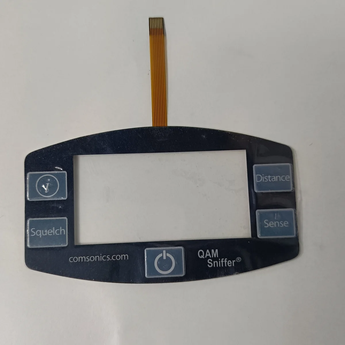
OEM teams evaluating custom capacitive touch panels can use the following route table before committing electrode artwork or tooling.
| Quick decision | Best fit | Primary constraint | First proof required |
|---|---|---|---|
| Conformal lamination of a flexible sensor | Cylindrical or gently curved covers with limited in-plane stretch | Adhesive must remain continuous and the film must lie against the lens without wrinkles | Laminated 3D sample mapped for touch delta and voids |
| Print flat, then thermoform | Repeatable formed film with decoration and sensors on one carrier | Local draw changes trace width, spacing, resistance and registration | Forming trial with strain grid, electrical coupons and fiducials |
| Film insert molding / in-mold electronics | Integrated plastic HMI with production tooling and fixed geometry | Printed materials must survive forming, trimming, heat, pressure and resin flow | Tool-produced part with post-form and post-mold electrical maps |
| Segmented rigid or hybrid sensors | Tight local corners, low volume, serviceable modules or mixed flat zones | Gaps between segments must not create a poor user interface | Functional mock-up of transitions and coordinate handoff |
Curved capacitive touch is a stack-level design problem
A curved touch surface changes the electric field and manufactured geometry together. A flat projected-capacitive matrix begins with regular transmit and receive electrodes; forming changes intersection spacing, electrode area and trace paths. The 2024 ACM Transactions on Graphics paper Capacitive Touch Sensing on General 3D Surfaces identifies regular electrode distribution as central to consistent sensitivity on complex shapes.
The controller measures capacitance, not curvature. Cover thickness, dielectric material, bond continuity, display distance, grounded hardware and trace length all change its electrical load. Firmware can compensate for bounded variation. It cannot repair a cracked trace, hidden void or displaced touch target.
Choose the sensing architecture explicitly. Self-capacitance buttons and mutual-capacitance touchpads have different routing constraints; a transparent display sensor also adds optical and resistance limits. The Custom Capacitive Touch Panel Design Guide provides the flat-panel foundation. Curved projects add surface mapping, forming and 3D inspection.
The final stack must be defined before electrodes are laid out
The controlling dimension is the complete dielectric and mechanical path from the user's finger to the sensing electrode. Cover-lens material and thickness matter, but so do decorative ink, hard coat, adhesive, sensor carrier, molded resin and any local air gap. Texas Instruments' CapTIvate design guide explains that low-dielectric air gaps weaken the touch signal and that overlay thickness and relative permittivity change electrode behavior.
Reference architecture for a display-backed curved interface:
Finger, glove or conductive stylus
                 ↓ local touch target
┌──────────────────────────────────────────────┐
│ Curved cover lens / formed decorated surface │
├──────────────────────────────────────────────┤
│ Continuous adhesive or optical bond          │  ← void and thickness control
├──────────────────────────────────────────────┤
│ Formed TX/RX sensor film or printed circuit   │  ← final-surface pitch and registration
├──────────────────────────────────────────────┤
│ Shield / dielectric gap / molded carrier      │  ← defined only when required
├──────────────────────────────────────────────┤
│ Display, backlight, chassis and nearby metal  │  ← noise and parasitic-capacitance sources
└──────────────────────────────────────────────┘
                 │ formed tail with strain relief
                 └── connector → touch controller → I2C/SPI/USB host
Dimension every active-area layer and transition. Nominal cover thickness is insufficient where forming thins the wall or adhesive pools near a concave feature. Conductive pigments and metallic decoration also require electrical review because they can shield the field. Supplier stack limits only screen a concept; a manufactured sample proves it.
Review the sensor with the display, backlight, chassis ground and controller location. The Projected Capacitive Touch Panel Technology overview covers the TX/RX principle; curved geometry modifies that architecture.
Select the manufacturing route from the final geometry and volume model
Developable shapes, including cylinders and cones, can accept a flexible film with little in-plane strain. Compound curves require stretch, compression, seams or relief. Geometry sets the route.
Conformal lamination bends an already fabricated circuit during bonding. It reduces conductor-forming damage, but makes adhesive placement critical. It fits mostly one-axis curvature supported by a shaped pressure nest; concave pockets and reverse transitions raise wrinkle and void risk.
Thermoformed printed film uses heat with pressure or vacuum to shape a printed polymer sheet. Pre-distorted artwork places electrodes and icons at their final coordinates. Local stretch can narrow or crack a conductor. Peer-reviewed 2026 work in Advanced Materials Technologies on 3D in-mold conductors shows nonuniform strain and material-dependent electrical response.
Film insert molding / in-mold electronics adds trimming and back-injection. Covestro's Film Insert Molding process shapes and trims a printed film before molding; the ink system must survive forming, heat and resin shear. Published material compatibility never creates a universal strain limit.
Segmented rigid or hybrid sensors reduce risk at sharp features, in low-volume programs or where modules need service. Packaging and zone transitions replace forming as the main design problem.
The Capacitive Touch Film and Foil Design Guide covers conductor and carrier choices. Large-Format Capacitive Touch Panel Design adds long-trace, display-noise and spatial-uniformity constraints.
Capacitive touch sensing on general 3D surfaces requires geometry-aware electrode compensation
One headline radius cannot release a curved touch design. Define local inside and outside radii, curvature direction, transitions, draw depth and compound-curvature zones. An identical nominal radius produces different strain on a cylindrical band, at a corner or beside a fixed trim edge.
Start with final A-surface CAD, map active zones in surface coordinates, then model deformation for the proposed tool. Compensate the flat artwork so final pitch, pad area and graphic alignment meet the drawing. The 2026 ETH Zürich surface-conforming sensing project demonstrates the method: generate conductors on the 3D object, then unfold them into 2D paths.
Keep narrow traces, connector pads and stiffener edges away from peak strain unless qualified there. Use gradual turns. Specify electrode pitch on the finished surface.
| Drawing variable | Why it changes performance | Failure if omitted | Required supplier output |
|---|---|---|---|
| Final A-surface CAD and datums | Establishes the touch and inspection reference | Graphics and sensor pass separately but miss after assembly | Marked 3D model and alignment method |
| Local radii and transitions | Sets bend and stretch distribution | Cracking, wrinkles or wall thinning | Zone-based formability review |
| Draw direction, depth and trim | Controls material flow | Artwork lands outside the target | Compensation file and fiducial map |
| Active boundary in surface coordinates | Defines resolved touch area | Edge dead zone or coordinate clipping | Final-surface electrode map |
| Final pitch and target size | Sets coupling and interpolation | Weak nodes or nonlinear tracking | Layout tied to controller and stack |
| Tail path and stiffener keep-out | Concentrates interconnect load | Intermittent tail or connector stress | Tail drawing, pinout and strain relief |
| Metal and display clearance | Changes loading and noise | False touch or reduced delta | Stack and grounding plan |
| Graphic-to-sensor registration | Links icon to electrical target | Touch reports under the wrong icon | Shared-datum tolerances |
Printing, forming and lamination need three separate registration controls
A curved assembly has three registration events: print-to-form, form-to-trim and sensor-to-cover or display. One final positional tolerance hides their separate variation. Give each event fiducials, datum transfer and an inspection state.
Print-to-form trials need stable sheet, controlled cure, a strain grid and electrical coupons oriented with and across the draw. Flat-sheet inspection cannot reveal post-form thinning or drift. Form-to-trim control locates the active area against edges, holes, bosses and the tail. Because a formed part can spring out of the tool, state whether inspection is free-state or in a defined nest. ISO 1101:2017 supplies form and location notation; the drawing must still assign limits.
Sensor-to-cover registration locates the electrical target under the visible icon. A shaped nest must support the lens without distorting it. Control adhesive thickness and coverage through every transition; a hidden void still changes the dielectric path.
Covestro's Film Insert Molding guidance distinguishes high-pressure forming where closer print positioning is needed from thermoforming where it is less critical. Actual capability remains specific to the film, print, tool, heat profile, draw and trim. Measure 3D profile, graphics, electrodes and tail in one coordinate system. Outer silhouette alone is insufficient.
Sensitivity tuning must follow the final mechanical assembly
Tune only after the formed, bonded and grounded assembly is stable. A flat coupon confirms continuity and communication; its thresholds are not release settings. Firmware comes last.
| Primary design evidence | Published conditions | Engineering implication |
|---|---|---|
| Texas Instruments CapTIvate Guide v1.83.00.08 | Example: 2 mm overlay, relative permittivity 3, about 1 mm electrode / ground spacing | Treat spacing as a controller-and-stack result, not a universal curved-panel rule |
| Microchip AN2934 (2020) | Self-capacitance guide: 4 mm plus cover thickness for electrode separation | Do not transfer a self-cap button rule to a mutual-cap matrix |
| Infineon Industrial Capacitive Touchscreen analysis | Simulated 1–4 mm covers with 5 mm and 10 mm pitch | Larger pitch can recover coupling but increase positional nonlinearity |
| Infineon AN85951 (accessed 2026) | Acrylic maxima vary by widget and generation: fourth-generation button 5 mm and touchpad 0.5 mm; fifth-generation button 18 mm and touchpad 3 mm | Never transfer a button or controller-generation limit to another architecture |
| Texas Instruments SLAA843A (2019) | CapTIvate SNR and noise across stated temperatures | Set margin from worst-case noise, not the room-temperature typical value |
Controller review should cover sensing mode, channels, electrode loading, shield support, glove / water strategy, scan latency, diagnostics, host interface and firmware ownership. Record baseline, touch delta, noise, signal-to-noise ratio, threshold margin and coordinate residual by node or zone.
Do not lower thresholds to hide an air gap, damaged conductor, ground coupling or distorted electrode. Correct the mechanics first. Then tune across the specified temperature, humidity, glove, water and user-grounding states.
Most curved-touch failures trace to geometry, bonding or parasitic loading
Curved-touch failures are usually spatial: a high-draw edge goes dead, coordinates jump at a transition, or moisture triggers one band. A panel-wide pass/fail threshold can hide the pattern. Inspect every zone.
| Failure symptom | Likely physical cause | Diagnostic evidence | Corrective direction |
|---|---|---|---|
| Dead zone after forming | Open trace, narrowed conductor or excessive local cover distance | Resistance map plus node delta before and after forming | Reroute from peak strain, change ink / carrier or reduce draw |
| Coordinate compression or jump | Final electrode pitch differs from the calibration map | Robotic or templated touch-position residuals | Update geometric compensation, then recalibrate |
| Weak band near a curve transition | Adhesive void, wall thinning or local electrode distortion | Cross-section / scan, bond inspection and raw-node map | Stabilize forming and bonding before threshold changes |
| False touch near display or chassis | Grounded metal or display noise raises parasitic loading | A/B test with final grounding states and powered display | Change spacing, shielding, routing or scan configuration |
| Drift during humidity exposure | Moisture changes the dielectric path or reaches a void | Baseline trend during the defined humidity profile | Improve sealing / bond control and retune only after correction |
| Intermittent tail | Forming or assembly load reaches the tail / stiffener junction | Continuity while fixtured through the assembly motion | Move the transition, add strain relief or change tail construction |
| Correct touch under the wrong icon | Graphic, electrode and trim use different datum chains | Overlay-to-electrode optical registration map | Establish one datum scheme and compensate each process step |
Reject capacitive sensing when the skin must flex repeatedly, conductive surfaces lack a qualified force-sensing architecture, re-entrant features prevent continuous bonding or field spread exceeds the required target. A segmented flat interface may also carry less risk when volume cannot support forming tools.
Validation must progress from flat coupons to powered final assemblies
A curved design needs checkpoints that separate material, forming, bonding, electronics and system effects. The OEM owns application requirements; suppliers assign each record before prototype release.
| Stage | Specimen and state | Measurements | Release question |
|---|---|---|---|
| Geometry review | Final CAD, stack and tool direction | Local radii, strain map, trim / tail access | Can critical traces avoid uncontrolled strain? |
| Flat coupon | Cured sheet | Line width, registration, resistance, opens / shorts | Is print stable before forming? |
| Formed sensor | Free-state and inspection nest | 3D profile, fiducials, resistance map | Did forming preserve geometry and continuity? |
| Trimmed / molded part | Final edges and support | Datums, tail exit, post-mold electrical map | Did trim or resin flow cause damage? |
| Laminated stack | Final cover, bond and display | Coverage, voids, active-area registration | Is the dielectric path continuous? |
| Powered assembly | Final controller and grounding | Baseline, delta, noise, SNR, linearity, residual | Does every zone pass? |
| Environmental sequence | Product-plan operating state | Before / during / after maps; IEC 60068-2-14:2023 and IEC 60068-2-78:2025 | Does exposure cause drift or separation? |
| EMC / ESD | Production enclosure and cables | Touch errors, resets, recovery; IEC 61000-4-2:2025 and IEC 61000-4-3:2020 | Does the complete HMI pass? |
| Pilot production | Cavities and lots | Dimension capability, diagnostics, defect pareto | Are limits stable? |
Infineon AN241195 Rev. A (2025) lists raw count, open / short integrity, electrode capacitance, shield capacitance, SNR and touchpad linearity for CAPSENSE production tests. Select equivalent diagnostics for another controller.
IEC 60068-2-14:2023 covers temperature change; IEC 60068-2-78:2025 covers steady-state damp heat. IEC 61000-4-2:2025 addresses ESD immunity, and IEC 61000-4-3:2020 addresses radiated RF immunity. The product authority selects severities and acceptance criteria.
Tie testing and validation planning to the drawing and keep prototyping and sample approval on production-intent materials.
If printed-coating separation is a control characteristic, ISO 2409:2020 supplies a cross-cut method within a limited scope. It is not a direct adhesion measurement and excludes coatings thicker than 250 µm (0.25 mm). Preserve every test map.
A complete RFQ defines geometry, stack, interface and acceptance criteria
A quote-quality package lets the supplier evaluate the curved surface without guessing which dimension or performance target controls. Include these inputs:
- final 3D CAD plus a dimensioned 2D drawing with datums, local radii and profile / location tolerances;
- active areas, icons and coordinate requirements mapped to the final surface;
- cover-lens or formed-film material, nominal thickness, coatings, decoration and color requirements;
- full adhesive, sensor, display, backlight, housing and nearby-metal stack;
- intended manufacturing route, expected volume and acceptable tooling approach;
- electrode type, touch mode, number of touches, target size and resolution / linearity requirement;
- glove, water, contaminant and user-grounding conditions;
- tail geometry, connector, pinout, controller preference, host interface and firmware ownership;
- operating / storage environment, chemical exposure and applicable EMC / ESD plan;
- cosmetic zones, permitted defects and all registration acceptance criteria;
- required prototype stages, first-article records, production diagnostics and change-control expectations.
Teams can send drawings for engineering review with the active area, cover lens, display stack, interface and operating environment. If the geometry and acceptance plan are already defined, request an engineering quote for a production-intent curved capacitive touch assembly.
Frequently Asked Questions
Can projected capacitive touch work through a curved cover lens?
Yes. A fixed, nonconductive curved lens can support projected capacitive touch when the sensor follows the surface, the bond line has no uncontrolled air gaps, and the electrode pattern is tuned with the final display, chassis and controller. Compound curvature raises forming and registration risk, so a powered 3D sample is required before release.
Is there a universal minimum bend radius for a curved capacitive touch sensor?
No. Minimum radius depends on film type and thickness, conductor material, trace orientation, adhesive, forming temperature, tool geometry and whether the sensor is bent once or flexed repeatedly. Specify local radii and the process stack, then qualify the most highly strained zones with formed electrical coupons and functional samples.
Does thermoforming change capacitive-touch electrode pitch?
Yes. Thermoforming redistributes a flat sheet over a 3D tool, so local stretch can change electrode spacing, area, conductor width and graphic position. The amount is spatially nonuniform. Define pitch on the final surface, use a strain or deformation map, pre-distort the flat artwork and verify the result in a datum-controlled inspection nest.
What is the best manufacturing route for capacitive touch sensing on general 3D surfaces?
Use conformal lamination for gently curved, mostly developable covers; thermoformed printed film for repeatable compound shapes; in-mold electronics when the circuit belongs inside a molded production part; and segmented rigid sensors for sharp features, low volume or serviceable modules. Final geometry, bonding access, tooling economics and inspection capability decide the route.
How do air gaps affect a curved capacitive touch panel?
An air gap adds a low-permittivity discontinuity between the finger and electrode, reducing and spatially varying the touch signal. On a curve, voids often collect near transitions where film or adhesive cannot conform. Inspect bond coverage on the actual shape and fix the mechanical process before compensating weak zones with lower firmware thresholds.
When should controller sensitivity be tuned?
Tune after the production-intent sensor, adhesive, cover, display, chassis ground, cable routing and controller are assembled. Record baseline, touch delta, noise, signal-to-noise ratio and coordinate residual by zone across the specified temperature, humidity, glove and water conditions. Flat-coupon settings are development aids, not final release values.
How should registration be inspected on a formed touch surface?
Use one datum scheme for the formed part, graphics, electrodes, trim features and tail. Inspect the part in the drawing-defined free or fixtured state, then report 3D profile, graphic-to-datum and electrode-to-graphic position in the same coordinate system. Outer-edge measurement alone cannot detect local active-area distortion.
When is capacitive touch not suitable for a 3D surface?
Avoid it when the skin must flex repeatedly, conductive decoration blocks the field, deep re-entrant geometry prevents continuous bonding, nearby metal cannot be controlled, or the required touch target is smaller than the achievable field spread. A segmented flat HMI, mechanical control or another sensing method can carry less technical and tooling risk.
References
- Palma, G., Pourjafarian, N., Steimle, J., and Cignoni, P. Capacitive Touch Sensing on General 3D Surfaces, ACM Transactions on Graphics 43(4), July 2024, DOI 10.1145/3658185.
- Ilic, A., et al. Retrofitting Existing 3D Objects with Surface-Conforming Capacitive Sensing, ACM SIGGRAPH 2026 project page.
- Texas Instruments. CapTIvate Technology Guide — Design Guide, version 1.83.00.08.
- Microchip Technology. Capacitive Touch Sensor Design Guide, AN2934, DS00002934B, 2020.
- Infineon Technologies. Industrial Capacitive Touchscreen Design Made Simpler.
- Infineon Technologies. AN85951: PSOC 4 and PSOC 6 MCU CAPSENSE Design Guide, accessed 2026.
- Infineon Technologies. AN241195: Manufacturing Test Recommendations for PSOC 4 CAPSENSE Designs, Rev. A, April 10, 2025.
- Texas Instruments. Sensitivity, SNR, and Design Margin in Capacitive Touch Applications, SLAA843A, revised March 2019.
- Covestro. Film Insert Molding: Creating Complex Components in a Single Step.
- ISO. ISO 1101:2017 — Geometrical Tolerancing, confirmed 2022.
- ISO. ISO 2409:2020 — Paints and Varnishes: Cross-Cut Test.
- IEC. IEC 60068-2-14:2023 — Change of Temperature and IEC 60068-2-78:2025 — Damp Heat, Steady State.
- IEC. IEC 61000-4-2:2025 — ESD Immunity and IEC 61000-4-3:2020 — Radiated RF Immunity.
- Advanced Materials Technologies. Molecular Inks for the Development of Complex 3D In-Mold Electronics, 2026.
Bring the drawing, stack and operating conditions
JASPER engineering will review the interfaces, open risks and evidence required for a production quote.