
A capacitive touch foil is a flexible sensor layer that places projected-capacitive electrodes behind a nonconductive touch surface. It is useful when an OEM needs a thin, lightweight or statically curved interface, but it is not automatically the best substitute for a rigid PCAP sensor. Choose the architecture only after fixing the cover lens, active area, electrode technology, adhesive, tail path, controller, display stack, curvature and operating environment. For optically critical flat displays, a rigid sensor may offer easier dimensional control. For keys or hidden controls, a printed sensor film may be simpler than a transparent XY touchscreen. These decisions belong in the system design for capacitive touch panels, not in the film drawing alone.
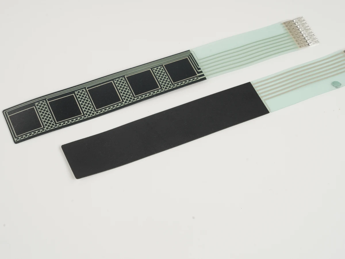
Quick decision: foil, rigid sensor, printed keypad or decorative film
The correct choice depends on what the layer must do. A transparent capacitive touch foil locates touches across an XY field; a printed sensor film implements defined keys, sliders or wheels; a rigid PCAP sensor holds its geometry on glass; and a decorative film supplies graphics without sensing.
| Architecture | What it contains | Best fit | Main integration limit |
|---|---|---|---|
| Transparent projected capacitive touch foil | Transparent Tx/Rx electrodes on flexible film, tail and controller | Rear-of-glass XY touch and some static curves | Bond uniformity, resistance, optics, noise and bend limits |
| Rigid PCAP sensor | Transparent electrodes on glass or another rigid substrate | Flat display stacks and precise registration | Higher mass; cannot conform after manufacture |
| Printed capacitive touch film keypad | Discrete keys, sliders or wheels on PET or flex | Hidden controls and backlit icons | Not continuous XY touch unless designed as a matrix |
| Decorative or graphic film | Legends, color, texture and optical windows | Visual finish and guidance | No touch-location function; conductive decoration can interfere |
Use the Custom Capacitive Touch Panel Design Guide for the broader cover-lens and assembly context. The rest of this guide focuses on the flexible sensor, its immediate stack and the controller interface.
Capacitive touch film, touch foil and decorative film are different parts
A capacitive touch film or capacitive touch foil is a flexible electrical sensor. In a transparent projected-capacitive design, patterned transmit and receive conductors form an XY matrix. The controller compares scanned nodes with a baseline and estimates touch position from the change.[^1]
A flexible capacitive touch sensor film can also mean a printed circuit with discrete buttons, a slider or a wheel. It may use printed silver/carbon or copper on FPC. It suits named control zones, not continuous coordinates. A rigid PCAP sensor uses the same sensing principle on a stable substrate, commonly glass, to simplify registration and flat optical lamination.
A decorative film carries legends, masks, texture or optical effects but no sensing circuit. It still changes the dielectric stack. Texas Instruments treats overlay ink, adhesive and transition materials as electrical “mechanicals” because they affect signal and parasitic capacitance.[^2] Metallic ink, conductive mirror coating and floating metal trim require electrical review.
How capacitive touch foil works in the complete stack
A projected capacitive touch foil is passive until a matched controller drives its electrodes. The complete touch path extends from the user’s finger through the cover stack, across the sensor matrix and into firmware that reports coordinates to the host.
Canonical anatomy and signal-flow diagram — front to back
User touch
    ↓
┌──────────────────────────────────────────────────────────┐
│ Cover lens / front panel: glass, PMMA or polycarbonate  │
├──────────────────────────────────────────────────────────┤
│ Optional decorative layer: legends, mask, optical finish│
├──────────────────────────────────────────────────────────┤
│ Uniform nonconductive bond: OCA or qualified PSA         │
├──────────────────────────────────────────────────────────┤
│ Flexible sensor substrate: patterned Tx/Rx electrodes   │
│ Active area → border traces → bonded or integral tail    │
└──────────────────────────────────────────────────────────┘
                  ↓ raw electrode signals
       Touch controller + tuned firmware
                  ↓ I2C, SPI or USB HID implementation
             Host processor / operating system

Adjacent system layers: shield/ground strategy → air gap or optical bond
→ LCD/TFT/OLED → chassis, power supply, antennas and enclosure
In mutual-capacitance PCAP, each transmit/receive crossing creates a coupling node. A finger changes the local field, and the controller interpolates position from multiple nodes; the grid does not output a USB coordinate by itself. See Projected Capacitive Touch Panel Technology for the sensing modes.
The cover, decoration, adhesive and substrate act as a dielectric stack. More thickness generally reduces signal; higher relative permittivity can recover part of it. Infineon lists 7.6–8.0 for standard glass, 3.2 for PET, 2.9–3.0 for polycarbonate and 2.8 for acrylic in its CAPSENSE model.[^3] The finished assembly still needs tuning and test data.
Sensor variants have different limits and sourcing inputs
Projected capacitive touch film does not identify the conductor, layer count or bend capability. The drawing must name the construction.
| Variant | Electrode/substrate concept | Optical role | Curvature behavior | Do not select it when |
|---|---|---|---|---|
| Transparent ITO-on-film XY sensor | ITO on PET or polymer film | Transparent | Supplier-approved static curve | Repeated tight flex lacks fatigue data |
| Silver or metal-mesh XY sensor | Fine conductive network on film | Transparent; pitch affects visibility | Construction-specific | Moiré, visibility or migration is untested in the final stack |
| Printed discrete sensor film | Printed conductors on PET | Opaque or translucent | Simple curves if designed for them | Continuous high-resolution XY touch is required |
| Copper FPC sensor | Etched copper on flex substrate | Usually opaque | Flexible routing; stack sets bend life | The active area must be transparent |
| Rigid glass PCAP | Transparent pattern on glass | Transparent, stable | Flat or rigid-preformed | The delivered sensor must conform to the housing |
A peer-reviewed silver-nanowire study identifies polymer adhesion and fine-pitch patternability as process risks.[^4] Request the offered conductor stack, patterning method, resistance limits, adhesion test and bend-test conditions.
Substrate and electrode pattern must be designed as one electrical system
The substrate controls flexibility and registration; the conductor controls transparency, resistance and routing. Balance touch signal against parasitic capacitance and noise.
For an XY capacitive touch film, pitch must suit the finger target, cover thickness, controller channels and interpolation. Infineon gives a 5–10 mm diamond pitch and 0.01–1 mm gap/bridge ranges for one single-layer example.[^1] These are scale references, not universal release dimensions.
Discrete keys start from another geometry. NXP advises that an electrode resemble the target finger area and warns that excessive area can increase noise and overlap adjacent zones.[^5] Its screen-printed example cites 0.018 in minimum trace width and 0.020 in spacing; transparent PCAP processes can work at another scale.
Conductor resistance matters along the full path. Renesas notes that ITO, silver and carbon pastes generally have higher resistance than copper and that long single-sided routing can reduce drive frequency or create location-dependent sensitivity.[^6] Check resistance and parasitic capacitance at the farthest node, including border trace, tail, connector and installed chassis.
Shielding is a tradeoff: it can reduce noise but also add parasitic capacitance and pull the field from the touch surface. TI uses electrode-to-ground separation of at least half the overlay thickness as a starting rule and favors a hatched pour when lower capacitance is needed.[^2] Verify that controller-specific rule on the released stack.
Adhesive, cover lens and decoration set the real sensing distance
Capacitive touch film adhesive must maintain a uniform, nonconductive bond line, wet both surfaces, survive the environment and preserve sensing distance.
An air gap weakens coupling, and a partial bond can vary sensitivity. Infineon recommends mechanical contact through nonconductive adhesive; Renesas warns that adhesive aging or assembly variation can increase sensing distance until a control becomes unresponsive.[^3][^6] Temporary tape is not representative of full-area production lamination.
Use optically clear adhesive (OCA) for a transparent full-area optical bond, or a qualified PSA when its optical, dielectric and environmental behavior fits. 3M’s OCA 817X sheet describes carrierless acrylic products at 25 µm and 50 µm and labels the data as typical, not specification values.[^7] Name the adhesive, thickness/tolerance, surface preparation, lamination method and cosmetic limits.
Nonconductive legends can sit above discrete keys, but icon shape should not dictate electrode shape. Conductive inks, mirror layers and floating metal can screen or distort the field.[^2][^3] Supply artwork, ink stack, coating location and surface resistance for mirror glass or metallic dead fronts.
The tail and controller determine whether “USB touch foil” is accurate
A bare foil terminates in a printed tail, bonded FPC, FFC or connector. A controller reads the electrodes; its board or bridge may expose I2C, SPI or USB.
Renesas describes film devices as electrode/wiring assemblies commonly connected by FPC/FFC to a controller board.[^6] NXP advises against creasing the tail.[^5] Specify tail exit, datum, length, contact orientation, stiffener, keep-out, installed bend path, strain relief and expected connector insertions.
“USB touch foil” should mean the assembly includes a controller or bridge. USB-IF’s HID class defines self-describing reports and touch-screen digitizer usages.[^8] Confirm descriptor, touch count, report rate, OS support, firmware update, power and cable length. Direct I2C can remove a bridge but shifts driver and firmware-management work to the OEM.
Tune with the released stack. Cover, adhesive, pitch, tail resistance, display noise, glove/water modes and chassis ground all change the signal window.
Curvature is safe only when the sensor, adhesive and tail share the same limit
A flexible sensor can follow a static curve, but “flexible” does not mean foldable or qualified for repeated bending. A planar foil conforms naturally to a cylinder; a compound surface adds in-plane strain and may wrinkle, lift or shift registration. Approve the 3D surface, laminate direction and process before tooling. See Capacitive Touch Design for Curved and 3D Surfaces.
Separate three radius values in the drawing:
- Sensor-body installed radius for the active film and border traces.
- Tail bend radius for the conductor stack, stiffener transition and connector approach.
- Lamination/forming radius imposed during assembly, which may be tighter than the final installed shape.
No single radius covers ITO-on-PET, silver nanowire, metal mesh, printed silver and copper FPC. Repeated-flex tests need direction, radius, angle, frequency, cycles, temperature and electrical/touch failure criteria. A static prototype is not dynamic-flex evidence.
Display, mirror and enclosure integration can dominate touch performance
Validate with the production display, supply, chassis, cable and firmware. Display switching noise can couple into PCAP electrodes and cause jitter, false touches or missed touches.[^1] LCD and TFT Integration With Capacitive Touch Panels is therefore a system decision.
For a PCAP touch foil behind mirror glass, identify the reflective coating and its conductivity. A front conductive layer can screen the field; one behind the sensor can alter baseline capacitance or carry noise. Any edge deletion, patterned coating or grounding decision depends on measured coating resistance and the full stack.
Evaluate moiré, mesh visibility, haze, color shift and reflections with the display operating. A loose sample over a light box does not reproduce a bonded LCD.
Keep regulators, LED power paths, antennas and fast digital lines away from the border and tail. Give metal a deliberate reference; verify bezel and gasket effects after final assembly.
Do not choose a flexible capacitive touch foil for every interface
A flexible foil is a poor default for dynamic folding without fatigue data, uncontrolled optical lamination, a conductive touch surface, or a controller that cannot support the electrode load and noise. Choose rigid PCAP when flatness and registration dominate, or printed discrete keys when continuous coordinates are unnecessary. Mechanical or resistive inputs may fit pressure actuation, conductive gloves, heavy water or mandatory tactile confirmation better.
Large format alone does not select foil. A 55-inch design changes channel count, border resistance, lamination, display noise and host behavior. Compare price only after the active area, stack, touch count, optics, controller and validation scope match.
Failure paths point back to the stack, not just firmware
Touch failures often appear in software but originate in the stack. Diagnose before increasing sensitivity globally.
| Symptom | Likely physical or electrical causes | Verification action |
|---|---|---|
| Missed touch across the area | Stack too thick, controller mismatch, low signal or shield coupling | Record raw signal/noise with the production lens |
| Weak edge or corner | Resistive border trace, poor tail bond, air gap or damage | Map nodes; measure far-node continuity/resistance |
| False touch as display content changes | Display switching noise or poor ground | Exercise high-transition images, brightness and power modes |
| Stationary-finger jitter | Low SNR, RF noise, unstable power or floating metal | Log coordinates/raw channels while exercising noise sources |
| Change after temperature/humidity | Adhesive movement, moisture, permittivity shift or baseline drift | Recondition the assembly and repeat its touch map |
| Bubbles, whitening or delamination | Contamination, adhesive mismatch, trapped air or expansion | Check defects, process settings and surface preparation |
| Intermittent tail | Crease, poor strain relief, stiffener damage or connector wear | Monitor continuity while flexing the installed route |
| False touch with water or glove | Wrong tuning mode, bridged electrodes or added sensing distance | Test each specified glove and water condition separately |
Preserve raw-channel logs, firmware, tuning, display image, supply mode, ground and environment for every reproduction.
Validation must use the released lens, display, controller and enclosure
Qualify the complete assembly. Before testing, define allowed misses, false touches, coordinate error, edge behavior, recovery and cosmetic limits.
| Validation block | Minimum production-representative inputs | Method or scope decision |
|---|---|---|
| Touch map and linearity | Released stack, firmware and active-area drawing | Test finger, glove, stylus, edge and multi-touch conditions |
| Display interaction | Production display, cable and power modes | Measure jitter, false and missed touches with worst image patterns |
| Optical quality | Bonded decorated stack and display | Apply ASTM D1003-21 where in scope; add moiré/cosmetic criteria[^9] |
| Adhesive/environment | Production surfaces and lamination | Expose to specified environment; inspect and repeat touch map |
| Static/dynamic curve | Installed radius, forming path and tail route | Measure resistance and touch through the bend sequence |
| ESD immunity | Complete powered equipment and cables | Use IEC 61000-4-2:2025 with product-defined levels/criteria[^10] |
| RF immunity | Equipment in representative modes | Apply IEC 61000-4-3:2020 and IEC 61000-4-6:2023 as required[^11] |
| Ingress/sealing | Final enclosure and every leak path | IEC 60529 applies to the enclosure, not loose film[^12] |
| Host/interface | Production host, cable and software | Verify enumeration, reports, suspend/resume, reset and recovery |
Connect the design review to testing and validation planning before the stack is frozen. Use prototyping and sample approval to preserve the approved lens, bond line, controller configuration and golden touch map rather than approving the film by appearance alone.
Project-input checklist for a touch-film RFQ
Send a controlled drawing package, not only a diagonal size. The supplier needs enough information to evaluate the sensor, cover lens, tail, controller and validation boundary together.
- Active area, view area, outer dimensions, border allowance and XY datum
- Required function: continuous XY touch, touch count, discrete keys, slider or wheel
- Cover-lens material, thickness, tolerances, surface treatments and decoration stack
- Display make/model, mechanical stack, air gap or optical bond, cable and grounding concept
- Sensor preference, transparency target, allowed visible pattern and optical acceptance criteria
- Adhesive family or required properties, thickness/tolerance, lamination process and cosmetic limits
- Static surface geometry or 3D CAD, installed radius, forming path and any repeated-flex requirement
- Tail exit, length, bend path, contact orientation, connector, stiffener, keep-outs and strain relief
- Controller/interface requirement: bare sensor, controller IC, I2C/SPI, or USB HID assembly
- Host OS/processor, cable length, power budget, driver ownership and firmware-update path
- Finger, glove, stylus, water/cleaning and palm-rejection requirements
- Operating/storage environment, ESD/EMC requirements, sealing target and service life conditions
- Required sample reports, raw data, tuning files, inspection criteria and change-control documents
When these inputs are ready, send drawings for engineering review. Include the active area, cover lens, display stack, interface and operating environment so the proposed construction can be reviewed as a system. For a production RFQ, request an engineering quote against the same controlled inputs.
Frequently asked questions
What is the difference between capacitive touch foil and a rigid PCAP sensor?
Capacitive touch foil puts electrodes on flexible film; rigid PCAP holds them on a stable substrate such as glass. Foil suits thin or statically curved integration. Rigid sensors simplify flatness, registration and optics.
Is capacitive touch film the same as a decorative film?
No. Touch film contains sensing electrodes and a controller connection. Decorative film carries legends, masks, texture or optical effects. It changes the dielectric stack, and conductive decoration can disturb sensing, but decoration alone does not locate touch.
How does an XY capacitive touch film detect position?
Transmit and receive electrodes form an XY matrix. The controller compares nodes with a baseline and interpolates the finger-induced change. Pitch, cover stack, noise and algorithms jointly determine performance.
Can capacitive touch foil work through thick glass or acrylic?
It can work through a qualified nonconductive cover, but no universal maximum thickness exists. Signal depends on sensing distance, permittivity, electrode geometry, controller, glove/water mode and noise. Tune and validate with the actual bonded stack.
Does a capacitive touch foil connect directly by USB?
Normally not. A tail connects the electrodes to a controller. Its board or bridge may expose USB HID, while embedded products often use I2C or SPI. Specify a bare sensor, matched controller or complete USB assembly.
What adhesive should be used for capacitive touch sensor film?
Use a uniform, nonconductive adhesive qualified for the surfaces, optics, environment and life. OCA is common for transparent full-area bonds, but product and thickness matter. Validate production lamination; temporary tape or an air gap is not equivalent.
Can projected capacitive touch film bend around a curved surface?
Many films follow a static developable curve, but the supplier must approve radius, forming path, conductor, adhesive and tail. Compound curvature and repeated flex add strain and fatigue. No generic bend radius covers ITO, silver mesh, printed silver and copper FPC.
Does a touch foil make the finished product waterproof?
No. A sensor may sit behind a sealed surface, but seams, gasket, tail exit, connector and vents remain leak paths. IEC 60529 classifies enclosure protection. Claim an IP code only after the complete product passes the applicable test.
References
[^1]: Infineon Technologies, Industrial Capacitive Touchscreen Design Made Simpler, PCAP construction, electrode geometry, controller interface and display-noise sections. https://www.infineon.com/assets/row/public/documents/30/59/infineon-industrial-capacitive-touchscreen-design-made-simpler-whitepaper-en.pdf [^2]: Texas Instruments, CapTIvate Technology Guide — Design Guide, mechanical stack, overlay, grounding and electrode-layout guidance. https://software-dl.ti.com/msp430/msp430_public_sw/mcu/msp430/CapTIvate_Design_Center/latest/exports/docs/users_guide/html/CapTIvate_Technology_Guide_html/markdown/ch_design_guide.html [^3]: Infineon Technologies, AN85951 — PSoC 4 and PSoC 6 MCU CAPSENSE Design Guide, overlay material, thickness and adhesive sections. https://documentation.infineon.com/psoc6/docs/epf1667481159393 [^4]: Y. Kim, C. Song, M. Kwak, B. Ju and J. Kim, “Flexible touch sensor with finely patterned Ag nanowires buried at the surface of a colorless polyimide film,” RSC Advances 5 (2015): 42500–42505. https://doi.org/10.1039/C5RA01657F [^5]: NXP/Freescale Semiconductor, AN3863 — Designing Touch Sensing Electrodes, Rev. 4, capacitive-film and electrode-pattern sections. https://www.nxp.com/docs/en/application-note/AN3863.pdf [^6]: Renesas Electronics, Capacitive Sensor Microcontrollers CTSU Capacitive Touch Electrode Design Guide, R30AN0389EJ0221 Rev. 2.21, June 29, 2026. https://www.renesas.com/en/document/apn/capacitive-sensor-microcontrollers-ctsu-capacitive-touch-electrode-design-guide [^7]: 3M, 3M Optically Clear Adhesive OCA 817X Series Technical Data, 2018. https://multimedia.3m.com/mws/media/631323O/3m-optically-clear-adhesive-8171x-series-tech-data-sheet.pdf [^8]: USB Implementers Forum, Device Class Definition for HID 1.11 and HID Usage Tables 1.7. https://www.usb.org/document-library/device-class-definition-hid-111 and https://www.usb.org/sites/default/files/hut1_7.pdf [^9]: ASTM International, ASTM D1003-21 — Standard Test Method for Haze and Luminous Transmittance of Transparent Plastics. https://store.astm.org/d1003-21.html [^10]: International Electrotechnical Commission, IEC 61000-4-2:2025 — Electrostatic Discharge Immunity Test. https://webstore.iec.ch/en/publication/68954 [^11]: International Electrotechnical Commission, IEC 61000-4-3:2020 — Radiated RF Electromagnetic Field Immunity Test and IEC 61000-4-6:2023 — Conducted RF Immunity. https://webstore.iec.ch/en/publication/59849 and https://webstore.iec.ch/en/publication/65586 [^12]: International Electrotechnical Commission, IEC 60529 — Degrees of Protection Provided by Enclosures (IP Code), consolidated edition. https://webstore.iec.ch/en/publication/2452
Final suitability depends on the released stack, controller, environment and product-level validation. Apply the limits in the cited component data to the selected construction.
Bring the drawing, stack and operating conditions
JASPER engineering will review the interfaces, open risks and evidence required for a production quote.