
A 32 inch PCAP touchscreen should be selected as an installed sensing system, not as a glass size. OEM teams need to freeze the active area, aspect ratio, electrode material and pitch, controller channel architecture, cover/display stack, edge routing, enclosure datums, interface and operating states together. Large format is practical when the controller and sensor preserve touch margin at the worst location and the bonded assembly remains flat, clean and mechanically unloaded. If those inputs are unknown, a quoted diagonal and interface are not enough to approve the design.
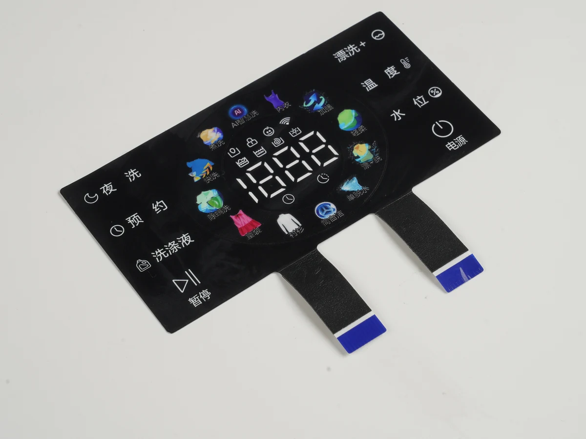
JASPER develops custom capacitive touch panels for OEM interfaces. This guide defines the evidence an engineer or buyer should request; it does not claim that one controller, conductor or bonding process fits every 32-inch program.
Large-Format PCAP Decisions at a Glance
The quickest safe decision is to treat sensor, controller, display, lens and enclosure as one qualification unit. A change to any one of them can alter the electrical baseline, noise coupling, optical result or mechanical stress.
| Decision | What must be fixed | Evidence to approve | Stop condition |
|---|---|---|---|
| Sensing geometry | Active area, aspect ratio, TX/RX allocation, pitch, edge zones | Sensor artwork review and raw-node map | Diagonal is known but line allocation is not |
| Transparent conductor | Material, sheet resistance lot range, pattern dimensions, optical target | Worst-path resistance calculation and optical sample | Material is named only as “ITO” or “mesh” |
| Controller | Usable channels, supported matrix, acquisition mode, report target, tuning ownership | Controller-vendor review using the actual stack | Controller is chosen from diagonal alone |
| Optical/mechanical stack | Lens, coatings, adhesive or air gap, sensor, display, gasket and datum scheme | Cross-section, tolerance stack and bonded cosmetic criteria | Flatness, load path or bond window is unspecified |
| Noise and interface | Display state, power source, grounding, shielding, cable and host protocol | Raw-data captures in worst powered states | Bench sensor is tuned without the production display |
| Validation | Operator, glove/water state, temperature, humidity, EMC and mechanical loads | Requirement-to-test matrix with pass/fail behavior | A component data sheet substitutes for system testing |
The broader Custom Capacitive Touch Panel Design Guide explains the controlled drawing package. Large-format work adds a stricter size-dependent electrical and mechanical review.
A Large Capacitive Touch Panel Is a Stack, Not a Single Part
A large capacitive touch panel normally includes a cover lens, transparent sensor electrodes, an adhesive or controlled air gap, a display interface, edge conductors, a flex tail, a controller and an installed ground/shield arrangement. “Touch panel,” “touch sensor” and “touchscreen” cannot be treated as interchangeable purchasing descriptions.
The cover lens carries cosmetic, impact, cleaning and operator-contact requirements. The sensor contains the coordinate grid; the controller measures it and reports touches. The display and enclosure remain part of the electrical system because switching, grounding, spacing and mechanical load change the controller input.
A coordinate PCAP sensor commonly uses mutual-capacitance intersections between transmit and receive electrodes. A controller may add self-capacitance, water handling, driven shielding or display synchronization, but those functions do not repair a weak stack. Microchip’s mXT2952TD supports mutual and self capacitance; its brief keeps size and performance statements configuration-dependent.[^1]
For a deeper explanation of sensing modes and coordinate generation, see Projected Capacitive Touch Panel Technology. The procurement boundary should then state whether the purchase is a bare sensor, lens-plus-sensor assembly, bonded display stack, controller board, firmware configuration or complete tuned HMI.
What Changes in a 32 Inch PCAP Touchscreen?
Increasing the diagonal length changes path resistance, electrode count or pitch, edge fan-out, flexible-tail geometry, lamination area, structural deflection and the number of locations that must meet the same touch criterion. A 32-inch drawing is not a scaled 7-inch drawing.
| Nominal size band | Typical engineering emphasis | What changes before the next band | Procurement implication |
|---|---|---|---|
| 2.4 to 5 inches | Compact stack and host integration | A 2.4 inch capacitive touch screen, 3.5 inch capacitive touch screen, 4 inch capacitive touchscreen or 5 inch capacitive touch screen can still fail through poor cover thickness, ground or routing; small size is not automatic margin | Confirm active area, overlay, controller and tail rather than buying by diagonal |
| 7 to 9 inches | Display coupling and enclosure integration | A 7 inch capacitive touch panel, 8 inch capacitive touch screen or 9 inch capacitive touch screen usually has enough area for edge uniformity and display-state testing to become visible system concerns | Require installed-display tuning and an edge/corner touch map |
| Around 15 inches | Resistance, line allocation and bonding process | A 15 inch capacitive touch screen increases path length, bond area and handling moment | Review conductor lot limits, channel map and lamination fixture |
| 27 to 32 inches | Large-format electrical and mechanical co-design | A 27 inch capacitive touch screen or 32 inch capacitive touch screen may need a different conductor, electrode pitch, controller topology, edge-routing process and support strategy | Quote the complete architecture; do not extrapolate a smaller qualified build |
These bands organize review work; they are not technology thresholds. Wide and tall 32-inch sensors need different TX/RX allocations, while coarse- and fine-pitch designs need different node budgets.
The first drawing review should compare active width and height, then identify the highest-resistance route, densest fan-out, least-supported lens region and strongest display disturbance.
Use an 11-Point Selection Matrix Before Requesting a Quote
An OEM can screen a large capacitive touch screen concept with eleven linked criteria. No row should be approved from a catalog adjective.
| Criterion | Good signal | Red flag |
|---|---|---|
| 1. Installed scope | Cross-section names every supplied and customer-supplied layer | “32-inch PCAP” is the entire specification |
| 2. Active geometry | Active, view and overall areas are dimensioned separately | Display diagonal substitutes for sensor geometry |
| 3. Conductor | Material, lot resistance range and optical acceptance are named | “High-transmission ITO” without measured limits |
| 4. Electrode pattern | Pitch, TX/RX allocation, edge zones and routing are reviewable | Proprietary pattern is offered with no compatibility review |
| 5. Controller | Channel map and acquisition mode are checked against the stack | A controller is selected only because a page lists a large size |
| 6. Lens and bond | Lens material, thickness, coatings, ink step and adhesive are frozen | Adhesive is “OCA” with no product, thickness or process |
| 7. Mechanics | Datums, support, gasket compression and allowable load are defined | The bezel is expected to force a warped stack flat |
| 8. Interface | Controller-board location, protocol, voltage and cable are owned | “USB or I2C” is left for production to decide |
| 9. Noise control | Display, power, ground and shield states are in the tuning plan | Tuning uses a sensor on a bench, away from its display |
| 10. Handling | Carrier, lift points, cleanliness and inspection lighting are specified | Operators lift a large bonded part by its flex tail |
| 11. Validation | Each requirement has a specimen state and failure criterion | “Pass IEC testing” appears without level or behavior |
Electrode Resistance and Controller Channels Set the Electrical Boundary
Large-format PCAP becomes difficult when the far end of an electrode no longer charges and settles with enough margin inside the controller’s acquisition window. Transparent conductor sheet resistance is only the material input; trace length, width, neck-downs, bus bars, crossovers, tail contacts and pattern geometry determine the path the controller must drive and measure. The supplier should calculate or measure the worst electrode path and identify its location on the artwork.
ITO combines transparency with established patterning. A 2023 peer-reviewed touch-panel study summarized conventional ITO above 90% optical transmittance and at 10–25 Ω/□, then evaluated metal mesh.[^2] Those figures are literature context, not a purchasing range. Mesh can reduce large-area resistance, but pitch, visibility, moiré, corrosion protection, continuity and inspection enter the decision. A 2019 review treats conductivity, transparency and mechanical behavior as coupled variables.[^3]
Channel count needs the same discipline. More channels can support a denser matrix, but active width, height, electrode pitch and controller allocation decide the required TX/RX combination. Microchip’s ATMXT3072M1 offers up to 112 configurable sensor lines. Its product brief gives a standard example of 17.65 inches at 16:9 with 5.5 mm electrode pitch and a separate ultrawide example up to 34 inches at 7:1 with 6 mm pitch.[^4] That is strong evidence that “supports 34 inches” does not mean “supports every 32-inch rectangle.”
Architecture can also change. Microchip describes an ATMXT3072M1 host/client solution for free-form widescreen sensors up to 42 inches that appears as one device to the host MCU.[^5] This is an example, not a default recommendation. The RFQ must identify one controller, a coordinated pair or another qualified topology, including synchronization, firmware and diagnostics ownership.
Request raw and processed data at center, edges and corners with the specified finger, glove, target and water states. A report rate needs its touch count, scan configuration, filters and host condition. The mXT2952TD, for example, lists 41 X lines, 71 Y lines and 2,911 nodes; its 21-inch example assumes 6.5 mm pitch.[^1]
Warpage, Lamination and Edge Routing Need Drawing-Level Controls
Large cover lenses and sensors magnify small process mismatches. The drawing should establish an inspection datum, permitted free-state shape, support points and the state in which flatness is measured. Forcing the assembly flat with bezel screws can transfer load into the display, adhesive, sensor or tail. Define the installed load path instead: supports carry the lens, the gasket seals within its compression window, and no clamp bears on an uncontrolled edge or active display region.
Optical bonding is a material-and-process system. The RFQ needs the adhesive family, thickness, chemistry, dielectric role, ink-step geometry, substrate surface energy, lamination method, debubble process, cleanliness class or particle criterion, cosmetic zones and rework rule. 3M’s touch-sensor guidance identifies acid chemistry, dielectric constant and ionic/moisture-driven corrosion as relevant OCA considerations.[^6] That makes “use clear adhesive” inadequate.
Supplier data must stay attached to the product and stack. The 3M OCA 817X sheet lists 25 µm and 50 µm variants and product-specific roller, vacuum and autoclave conditions. It reports no appreciable bubbles, delamination or whitening after 800 hours at 65°C/90% RH for three stated LCD-glass/8172CL/polymer constructions.[^7] These are not process settings or life claims for another assembly.
Edge routing must be reviewed before the cosmetic border is frozen. Every TX/RX line needs a controlled path to the tail or controller. Narrowing the border can force tighter line/space, more crossovers or a different deposition process. Document resistance by route, insulation between crossings, guard or shield ownership, bond-pad metallurgy, tail exit, bend keep-out and strain relief. The flex should not become a lifting handle.
Large parts need a rigid carrier, defined lift locations, protected tail storage and inspection lighting for particles, Newton rings, bubbles, scratches and coating nonuniformity. Shaped lenses need a dedicated Capacitive Touch Design for Curved and 3D Surfaces review rather than flat-panel tolerances.
Display Noise, Grounding and Interface Choices Must Be Validated Together
The production display is an electrical aggressor, not a passive background. Infineon documents how LCD switching couples through capacitance into nearby PCAP electrodes and can produce coordinate jitter, false touches or failure to recognize a real finger.[^8] Larger physical area does not prove worse noise by itself, but it creates more electrode area, longer routes and more locations where stack spacing or ground return can vary.
Build a noise-state matrix before tuning: display patterns and brightness extremes, every production supply, grounded and battery states, communication activity, nearby aggressors, wet/glove modes and enclosure states. Capture baselines, raw-node noise and touch deltas at fixed locations. Texas Instruments notes that capacitive touch systems can measure changes on the order of a picofarad or less.[^9]
| Observed symptom | Likely mechanism to isolate | Evidence to request |
|---|---|---|
| Stationary-finger jitter | Display coupling or unstable reference | Raw-node capture by display pattern and power state |
| False edge touch | Edge route, bezel load, moisture or shield termination | Location-tagged data before/after enclosure assembly |
| Missed touch at far corner | High path load, stack variation or filter threshold | Worst-electrode resistance and touch delta map |
| Reset or latch during RF/ESD | Interface, power or protection path | Controller log and recovery at the specified IEC 61000-4-2 or IEC 61000-4-6 state |
The ground and shield drawing should show what connects to chassis, digital ground, controller reference and display frame, and where those connections occur. Avoid a vague “add shield” action: a shield changes parasitic capacitance and may reduce touch signal if its placement and drive are wrong. Display-refresh synchronization, supported by controllers such as the mXT2952TD, can help move acquisition away from repeatable display disturbances, but it does not repair an unstable mechanical stack or an uncontrolled return path.[^1]
Choose the host interface after controller-board location and cable topology are known. I2C, SPI and USB HID create different voltage, grounding, connector, software and diagnostic requirements. Freeze firmware configuration, production programming, recovery and raw-data ownership. LCD and TFT Integration With Capacitive Touch Panels should be reviewed whenever the display or bond changes.
Validate the Installed Assembly, Not a Loose Sensor
A large capacitive touch panel should pass functional, optical, environmental, EMC and mechanical acceptance in its production-like enclosure with the production display, power supply, cable, ground and software. Component qualification is useful evidence, but it cannot represent the final coupling paths or stresses.
| Validation block | Specimen state | Measure or observe | Acceptance input |
|---|---|---|---|
| Touch map | Installed; all display/power states | Missed/false touches, coordinates, edge/corner behavior, touch count | Target size, operator, glove, water state, allowable error and recovery |
| Optical | Bonded stack; defined lighting and viewing geometry | Haze, transmittance, bubbles, particles, Newton rings, mura and coating uniformity | Cosmetic zones, instrument/method and numerical limits |
| Thermal/humidity | Powered and unpowered states as required | Baseline drift, bond appearance, corrosion, touch recovery and display effects | Temperature/RH profile, dwell, cycles, recovery and pass behavior |
| EMC/ESD | Production enclosure, cables and power | False/missed touch, reset, latch-up, coordinate drift and recovery | Phenomenon, level, dwell, performance criterion and permitted recovery |
| Mechanical | Installed supports and packaging states | Glass/sensor damage, bond shift, tail damage and post-test function | Shock/vibration/handling profile, axes, mounting and inspection |
ASTM D1003-21 provides haze and luminous-transmittance procedures for planar transparent plastics; the specimen, conditioning and method still need to be stated.[^10] IEC 61000-4-2:2025 covers operator-originated ESD immunity, IEC 61000-4-3:2020 covers radiated RF fields not in close proximity, and IEC 61000-4-6:2023 covers conducted RF disturbances from 150 kHz to 80 MHz through applicable cables.[^11][^12][^13] These are basic test methods. The relevant product requirement must select applicability, level and performance criteria.
For environmental and handling work, IEC 60068-2-14:2023 addresses specified temperature changes, IEC 60068-2-78:2025 addresses steady high humidity without condensation, and IEC 60068-2-27:2008 addresses prescribed mechanical shocks.[^14][^15][^16] Do not paste a standard number into an RFQ without the specimen state, severity, duration, axes and allowed post-test behavior.
Plan testing and validation planning before tooling. Use prototyping and sample approval to separate sensor/controller feasibility, bonded appearance and production-intent enclosure approval instead of asking one attractive sample to prove every requirement.
Run a Six-Step RFQ and Approval Process
The buyer process should preserve technical ownership from concept through release.
- Freeze the use case. Define operator, touch target, glove/water conditions, orientation, display content, environment and required recovery from disturbance.
- Issue one controlled stack drawing. Dimension overall, active and view areas; lens, coatings, ink, adhesive, sensor, display gap, tail, connector, bezel, gasket, supports and datums.
- Request the electrical architecture. Require conductor material and lot limits, worst-path resistance, TX/RX map, controller topology, interface, firmware ownership and raw-data access.
- Review manufacturing evidence. Approve the bond process window, carrier/fixture concept, cosmetic zones, edge-routing capability and traceable material list.
- Tune production-like samples. Use the final display, supply, ground, enclosure and intended software states. Record configuration versions and raw-node evidence.
- Close a requirement-to-test matrix. Link every drawing and performance requirement to a method, specimen count, pass criterion, report and change-control trigger.
Disqualifying red flags include an unnamed controller; no channel map; “any OCA” on the bill of materials; no flatness datum; no worst-case display state; a flex tail used to handle the panel; a cosmetic limit with no inspection method; or a claim of IEC compliance with no level and performance criterion.
The RFQ package should include: active and view dimensions; cover-lens CAD; display model and mechanical drawing; cross-section; mounting and gasket scheme; tail exit and connector; controller/host boundary; interface voltage and protocol; operating environment; touch/glove/water requirements; optical criteria; cosmetic zones; validation matrix; annual volume assumptions; revision control; and golden-sample approval rules.
When Large-Format PCAP Is Not the Right Choice
Large-format PCAP is a poor fit when the project cannot provide a stable dielectric stack, controlled grounding, compatible controller architecture or production-like tuning. It may also be the wrong primary control for a safety function that requires tactile confirmation or deterministic operation under heavy standing water, contamination or gloves outside the validated sensing envelope.
Infrared, resistive, optical or mechanical controls can be stronger alternatives when the required input object is nonconductive, the cover stack is highly variable, a very large display needs field-serviceable touch hardware, or the operating environment defeats capacitive margin. The decision should compare installed requirements, not assume PCAP is superior because it supports a clean glass front.
Frequently Asked Questions
Can a 32 inch PCAP touchscreen use one controller?
Sometimes, but diagonal alone cannot answer the question. The controller must support the required TX/RX allocation, aspect ratio, electrode pitch, conductor load, acquisition mode and report behavior. A 32-inch 16:9 sensor may require a different architecture from a 32-inch ultrawide sensor, including a coordinated host/client controller design.
Is metal mesh always better than ITO for a large capacitive touch sensor?
No. Metal mesh can reduce long-path resistance, while ITO offers established transparent-electrode processing. The choice must also account for optical transmission, haze, line visibility, moiré, corrosion protection, pattern continuity, bend behavior, controller compatibility and supplier process control. Approve measured samples over the intended display.
How should electrode resistance be specified for a 32-inch panel?
Specify the conductor material and lot range, then require maximum resistance for the worst complete electrode path on the released artwork, including neck-downs, bus bars, crossovers, pads and tail contacts. Record the measurement method, temperature, test points and allowed lot variation; sheet resistance alone is insufficient.
Does a thicker cover lens only require higher sensitivity?
No. Lens material and thickness change the dielectric stack, while coatings, adhesive, air gaps, ink steps, water, gloves and display noise affect usable margin. The controller, sensor pattern and complete stack must be reviewed and tuned together. Mechanical load and optical requirements may become limiting before nominal sensitivity does.
Should a large PCAP sensor be tuned before optical bonding?
Early loose-stack tuning can confirm feasibility, but final tuning must use the production-intent bonded stack, display, enclosure, power, ground and cable. Bond thickness, display spacing and mechanical support change capacitance and noise. Preserve raw data and configuration versions from both stages rather than treating early tuning as production approval.
What causes false touches near the edge of a large capacitive touch screen?
Likely causes include edge-electrode geometry, long or mismatched routes, display or cable coupling, shield termination, bezel or gasket loading, moisture paths and an incomplete edge calibration. Diagnose with location-tagged raw-node captures across display, power, mechanical and wet/dry states before changing firmware filters.
Which tests belong in a large-format PCAP validation plan?
Include installed touch mapping, display/power noise states, optical inspection and measurement, temperature change, steady humidity where relevant, ESD, conducted and radiated RF immunity, mechanical shock or vibration, cleaning exposure and post-test recovery. Select levels and pass criteria from the end product requirement, not from the touch panel alone.
What information is required for an accurate large-format PCAP quote?
Provide active and view areas, overall geometry, cover-lens CAD, display model, complete stack, mounting datums, gasket and bezel loads, conductor preference, controller/interface boundary, tail and connector, operator and touch targets, glove/water states, environment, optical limits, validation matrix, volume assumptions and revision-controlled approval evidence.
Project-Input Checklist
Before releasing a 32 inch PCAP touchscreen for quotation, confirm that the package contains:
- Active area, view area, overall outline, aspect ratio and orientation
- Cover-lens material, thickness, coatings, print, cutouts and cosmetic zones
- Sensor material, TX/RX concept, edge-routing space, tail and connector
- Display model, optical bond or air gap, power states and ground/frame details
- Controller location, architecture, interface, firmware and diagnostics ownership
- Enclosure datums, supports, gasket compression, bezel loads and handling carrier
- Operator, touch target, glove, water, cleaning and operating environment
- Optical, functional, EMC, environmental and mechanical acceptance matrix
- Prototype stages, golden-sample rules, revision history and change-control triggers
Use this package to send drawings for engineering review. Include the active area, cover lens, display stack, controller interface and operating environment so the review can test the coupled design assumptions. When the architecture and acceptance boundary are clear, request an engineering quote for the defined scope.
References
The cited component and material examples define the conditions for their specific parts. Select the final stack against the project requirements; an example part is not a default bill of materials. Technical references were reviewed on August 24, 2026.
[^1]: Microchip Technology, mXT2952TD 1.0 maXTouch 2911-node Touchscreen Controller Product Brief, 2019. https://ww1.microchip.com/downloads/aemDocuments/documents/OTH/ProductDocuments/DataSheets/mXT2952TDTouchscreenControllerProductBrief.pdf [^2]: S. Yuan et al., “Fabrication of Flexible and Transparent Metal Mesh Electrodes Using Surface Energy-Directed Assembly Process for Touch Screen Panels and Heaters,” Advanced Science, 2023, DOI 10.1002/advs.202304990. https://doi.org/10.1002/advs.202304990 [^3]: H. B. Lee et al., “Flexible Transparent Conducting Electrodes Based on Metal Meshes for Organic Optoelectronic Device Applications: A Review,” Journal of Materials Chemistry C, 2019, DOI 10.1039/C8TC04423F. https://doi.org/10.1039/C8TC04423F [^4]: Microchip Technology, ATMXT3072M1 Family Product Brief, 2025. https://ww1.microchip.com/downloads/aemDocuments/documents/HMID/ProductDocuments/ProductBrief/ATMXT3072M1_Family_Product_Brief_DS40002626B.pdf [^5]: Microchip Technology, “Microchip Expands maXTouch M1 Touchscreen Controller Series for Broader Display Size Coverage,” January 27, 2026. https://www.microchip.com/en-us/about/news-releases/products/microchip-expands-maxtouch-m1-touchscreen-controller-series [^6]: 3M, “Technical Resources for Optically Clear Adhesives,” accessed August 24, 2026. https://www.3m.com/3M/en_US/optical-solutions-us/applications/displays/optically-clear-adhesives/technical-resources/ [^7]: 3M, Optically Clear Adhesive OCA 817X Series Technical Data, 2018. https://multimedia.3m.com/mws/media/631323O/3m-optically-clear-adhesive-8171x-series-tech-data-sheet.pdf [^8]: Infineon Technologies, Industrial Capacitive Touchscreen Design Made Simpler, 2022. https://www.infineon.com/assets/row/public/documents/30/59/infineon-industrial-capacitive-touchscreen-design-made-simpler-whitepaper-en.pdf [^9]: Texas Instruments, CapTIvate Technology Guide: Design Guide — Noise Immunity, accessed August 24, 2026. https://software-dl.ti.com/msp430/msp430_public_sw/mcu/msp430/MSPWare/3_20_00_37/exports/MSPWare_3_20_00_37/captivate/docs/users_guide/html/ch_design.html [^10]: ASTM International, ASTM D1003-21: Standard Test Method for Haze and Luminous Transmittance of Transparent Plastics, 2021. https://store.astm.org/d1003-21.html [^11]: IEC, IEC 61000-4-2:2025 — Electrostatic Discharge Immunity Test, 2025. https://webstore.iec.ch/en/publication/68954 [^12]: IEC, IEC 61000-4-3:2020 — Radiated, Radio-Frequency, Electromagnetic Field Immunity Test, 2020. https://webstore.iec.ch/en/publication/59849 [^13]: IEC, IEC 61000-4-6:2023 — Immunity to Conducted Disturbances Induced by Radio-Frequency Fields, 2023. https://webstore.iec.ch/en/publication/65586 [^14]: IEC, IEC 60068-2-14:2023 — Change of Temperature, 2023. https://webstore.iec.ch/en/publication/71503 [^15]: IEC, IEC 60068-2-78:2025 — Damp Heat, Steady State, 2025. https://webstore.iec.ch/en/publication/82357 [^16]: IEC, IEC 60068-2-27:2008 — Shock, 2008. https://webstore.iec.ch/en/publication/514
Bring the drawing, stack and operating conditions
JASPER engineering will review the interfaces, open risks and evidence required for a production quote.