
Touch-panel EMI and ESD performance depends on the complete coupling and return path through the sensor, display, flex, ground, enclosure, protection network, controller, firmware, and host response.
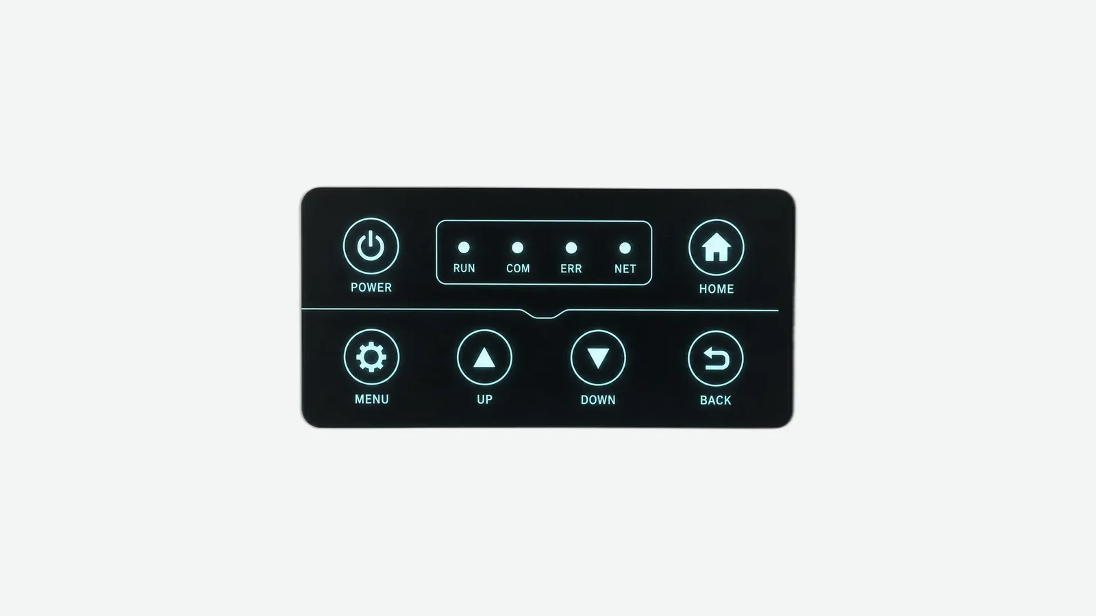
Start With the Interference Path, Not the Shield
A capacitive sensor measures small changes in an electric field. The installed HMI surrounds that measurement with LCD timing, backlight current, DC/DC conversion, chargers, radios, motors, external cables, enclosure metal, and human contact. A shield can help one path and create a new capacitance or return-current problem elsewhere. “Add a shield” is therefore not a design decision until the path is known.
Use one row per physical path:
SOURCE / EVENT
ENTRY POINT
(power port, cable, bezel seam, cover surface, display tail)
COUPLING PATH
(conductive, capacitive, inductive, radiated, common impedance, arc)
SENSITIVE NODE
(electrode, flex trace, controller reference, reset, supply, host link)
OBSERVABLE FAILURE
(false touch, missed touch, drift, reset, lockup, damage)
CONTAINMENT + EVIDENCE
(layout, return, shield, filter, protection, firmware state, raw data)
Texas Instruments uses the same layered principle in its TIDM-CAPTOUCHEMCREF work: hardware controls, touch-peripheral features, and signal processing operate together. TI’s reported reference-design performance belongs to that exact circuit, firmware, setup, and specimen. It is not evidence for another controller, a JASPER assembly, or finished OEM equipment.
The path model also separates symptoms that look alike. A missed touch can come from reduced sensor margin, a controller reset, a frozen host link, or an intentionally inhibited input. A useful record names the affected channel, controller state, host state, display state, disturbance time, and recovery—not just “touch failed.”
Failure classes to define before testing
| Class | Observable behavior | Project decision needed |
|---|---|---|
| Normal | Valid touches register; no false input occurs | No special response |
| Temporary degradation | Declared latency or sensitivity change exists only during exposure | Maximum duration and operator feedback |
| Controlled inhibition | Input is blocked because the measurement is unreliable | Safe machine state, visible indication, and recovery rule |
| Recoverable fault | Controller or touch function restarts without an unsafe command | Supervision, logging, and return-to-service rule |
| Unacceptable | False command, stuck input, corrupted configuration, damage, or unsafe state | Stop condition and corrective action |
A false command is often more serious than a missed command, but the equipment risk analysis must decide. Neither IEC 61000-4 nor a touch-controller manual can make that application decision.
Separate EMI Phenomena From the ESD Event
“EMC testing” is not one stimulus. Radiated RF, conducted RF, electrical fast transient/burst, and ESD create different paths. Combining them into one pass/fail line hides the information needed to correct a failure.
| Phenomenon | Current IEC basic method | Typical entry question | Touch-system observations |
|---|---|---|---|
| Electrostatic discharge | IEC 61000-4-2:2025 | Where can a user-originated discharge strike, arc, couple, and return? | False or missed input, reset, lockup, communication loss, permanent damage |
| Radiated RF field | IEC 61000-4-3:2020 | Which electrodes, traces, cables, apertures, or loops receive an external field? | Channel-specific shifts, coordinate error, false input, host upset |
| EFT/burst | IEC 61000-4-4:2012 | How do repetitive fast transients enter supply, signal, control, or earth ports? | Bursts of false input, resets, display upset, communication errors |
| Conducted RF | IEC 61000-4-6:2023 | Which connected cable carries RF current into the reference or sensing system? | Common channel movement, touch-dependent noise, threshold crossings, recovery errors |
IEC 61000-4-2:2025 defines equipment, setup, procedures, and calibration for reproducible ESD immunity work. IEC 61000-4-3:2020 addresses radiated fields from RF sources that are not in close proximity. IEC 61000-4-4:2012 covers repetitive burst applied to supply, signal, control, and earth ports. IEC 61000-4-6:2023 covers cable-coupled RF disturbances, principally from 150 kHz to 80 MHz.
Those documents are basic test methods. The applicable product or family standard decides which methods apply, along with severity, modulation, dwell, cable arrangement, mounting, operating mode, and performance criteria. A stable ESD demonstration cannot prove conducted-RF immunity. A clean bench supply cannot clear a cable-borne RF path.
Build Capacitive Touch Noise Immunity Around Signal Margin
Capacitive touch noise immunity is the ability to preserve valid decision margin and controlled behavior while disturbances alter electrodes, traces, references, power, or timing. A calm average count is not enough. The review needs the distributions for untouched baseline, valid touch signal, disturbance movement, adjacent-channel response, threshold, hysteresis, and post-event recovery.
| Evidence channel | What to retain | What it can reveal |
|---|---|---|
| Raw or minimally processed sensor values | All active and adjacent channels with timestamps | Local coupling versus common movement |
| Baseline and compensation state | Baseline value, update timing, freeze/restart conditions | Drift, bad recalibration, or post-event offset |
| Decision state | Threshold, hysteresis, debounce, touch/no-touch/fault output | Whether firmware masks or creates the visible symptom |
| Controller health | Reset reason, watchdog, configuration checksum, scan mode | Reset mistaken for a missed touch |
| System state | LCD pattern, brightness, charger, motor, cable, host command | Correlation with the actual source |
Renesas describes a useful conducted-noise mechanism in its 2024 CTSU guide. When circuit ground is not tied to earth, interference can move the board as common mode; a person capacitively coupled to earth then injects that disturbance through the finger-to-electrode path. Noise near the sensing waveform or its harmonics can produce larger measurement movement. This explains why a panel may appear stable untouched, then fail only when a person touches it while a charger or cable is connected.
Onsemi’s TND6033/D similarly identifies chargers, antennas, display integration, and ground loading as sources of false or phantom input in projected-capacitive systems. “Charger noise” is not one number. Adapter topology, protective-earth state, output cable, Y-capacitance, load, host grounding, and the user’s coupling all change the path.
Firmware can reject an improbable pattern, change sensing frequency, filter counts, add debounce, or inhibit input. It cannot shorten a long ESD return, move a flex away from a backlight converter, or stop common-impedance current in the controller reference. A higher threshold may suppress false input while breaking a gloved or edge touch. A longer filter may hide a burst while adding unacceptable latency. Any firmware correction needs before-and-after evidence for valid touch, no-touch, adjacent response, timing, and recovery.
Environmental tuning is a separate test dimension. Water films and gloves alter the electric-field boundary even without electrical interference; the water and glove tuning guide should own those state definitions. The immunity plan should still include each required wet or gloved state rather than treating dry-finger performance as a substitute.
Touch Panel Grounding Must Define Reference and Return
Touch panel grounding fails when one GND label is expected to serve six different jobs. Draw controller reference, digital/power return, display frame, cable shield, chassis, protective earth, and protection return as separate conductors before showing their intentional connections.
Touch electrodes → controller reference
Controller supply return · intentional network
Display/backlight return · (location and impedance controlled)
Cable shield → chassis entry
ESD protector → designated return
Chassis / bezel → protective earth? · project-dependent
A switching-load return shared with the controller can move the measurement reference. A floating bezel can become a variable coupling plate. A shield tied through a long narrow trace may carry fast current through the sensing region. A display frame bonded at an incidental screw can change when paint thickness, fastener torque, gasket compression, or service state changes.
Choose the structure by its electrical role
| Structure | Intended role | Required drawing information | When it is not the best choice |
|---|---|---|---|
| Passive grounded shield | Intercept electric-field coupling and reference an exposed region | Coverage, hatch/solid geometry, spacing, termination, return path, continuity | Not best when added parasitic capacitance destroys touch margin or its return injects noise |
| Driven shield | Follow a controller-supported waveform to reduce selected loading or coupling | Controller pin, waveform, permitted load, geometry, timing, emissions review | Not best when the controller does not support it, the load is excessive, or emissions worsen |
| Guard electrode/region | Detect or control a defined non-target condition | Sensed state, geometry, channel, firmware action, threshold | Not a universal EMI barrier and not a substitute for chassis current control |
| Chassis or bonded bezel | Carry structural or disturbance current outside sensitive reference paths | Material, finish, seams, fasteners, contact method, inspection | Not best when proximity loads the sensor or the bond cannot be controlled in production |
| Shielded flex/cable region | Reduce coupling along a routed interconnect | Layer, reference, coverage, connector pins, termination at each end | Not best when termination creates a loop or the shield is connected to an unsupported driven output |
Microchip AN2934 distinguishes passive shields held at a fixed potential from active or driven shields that follow the electrode waveform. Both alter the electric field. A grounded plane may improve isolation yet increase parasitic capacitance and reduce sensitivity. A driven structure may preserve sensitivity but adds controller-specific load, stability, timing, and emissions constraints.
Infineon AN85951 likewise treats ground, shield, guard, routing, external components, SNR, and tuning as connected decisions. Exact trace dimensions and clearances in that document belong to the documented PSoC/CAPSENSE conditions. They should not be copied into another controller design without checking that controller’s acquisition method and load limits.
The practical rule is simple: every conductive structure needs a named reference, current path, continuity requirement, and retuning trigger. If the review cannot state those four items, the shield concept is not ready for release.
How Display Noise Reaches a Capacitive Sensor
The LCD and touch sensor share a physical aperture, so display noise near a capacitive sensor can couple through electrode overlap, the display frame, FPC tails, high-speed interfaces, backlight conversion, or shared return impedance. Validate real display states rather than a static image on a development bench.
Record at least:
- display model and revision;
- frame/backplate material and bond;
- display and touch FPC position after enclosure closure;
- interface and cable route;
- image transitions and refresh modes;
- backlight converter location and switching state;
- brightness-control method and load;
- startup, sleep, wake, fault, and hot-plug states where allowed;
- touch scan mode and any controller-supported synchronization.
Infineon AN234185 discusses an ITO shield between display electronics and the touch sensor when display coupling dominates. That construction is not automatically correct. The shield must cover the vulnerable electrode and trace region, connect to the intended reference, stay within optical and manufacturing limits, and preserve sensor margin. Added ITO resistance, layer capacitance, optical stack changes, and tail termination can alter the result.
Flex routing deserves its own controlled drawing. Keep sensor lines short where the selected controller requires it; separate them from display clocks, backlight PWM, DC/DC switch nodes, LEDs, radios, motors, and high-current conductors. Where crossing cannot be avoided, review coupling geometry rather than relying on a generic distance. Microchip’s maXTouch layout guidance separates grounded and driven-shield functions and treats X/Y routes, edge ESD structures, FPC coverage, and loop area as architecture-specific controls.
Use industrial control interfaces as one equipment context: an operator panel may combine a PCAP sensor, LCD, 24 V input, isolated communications, long harnesses, relays, and a metal door. The exact link may remain 404 until the planned route is published; its purpose here is contextual navigation, not evidence.
A display or FPC alternate is an EMC change even when active area and connector pitch match. Different frame bonds, cable layers, driver timing, backlight topology, and assembly pressure can change both noise coupling and baseline capacitance.
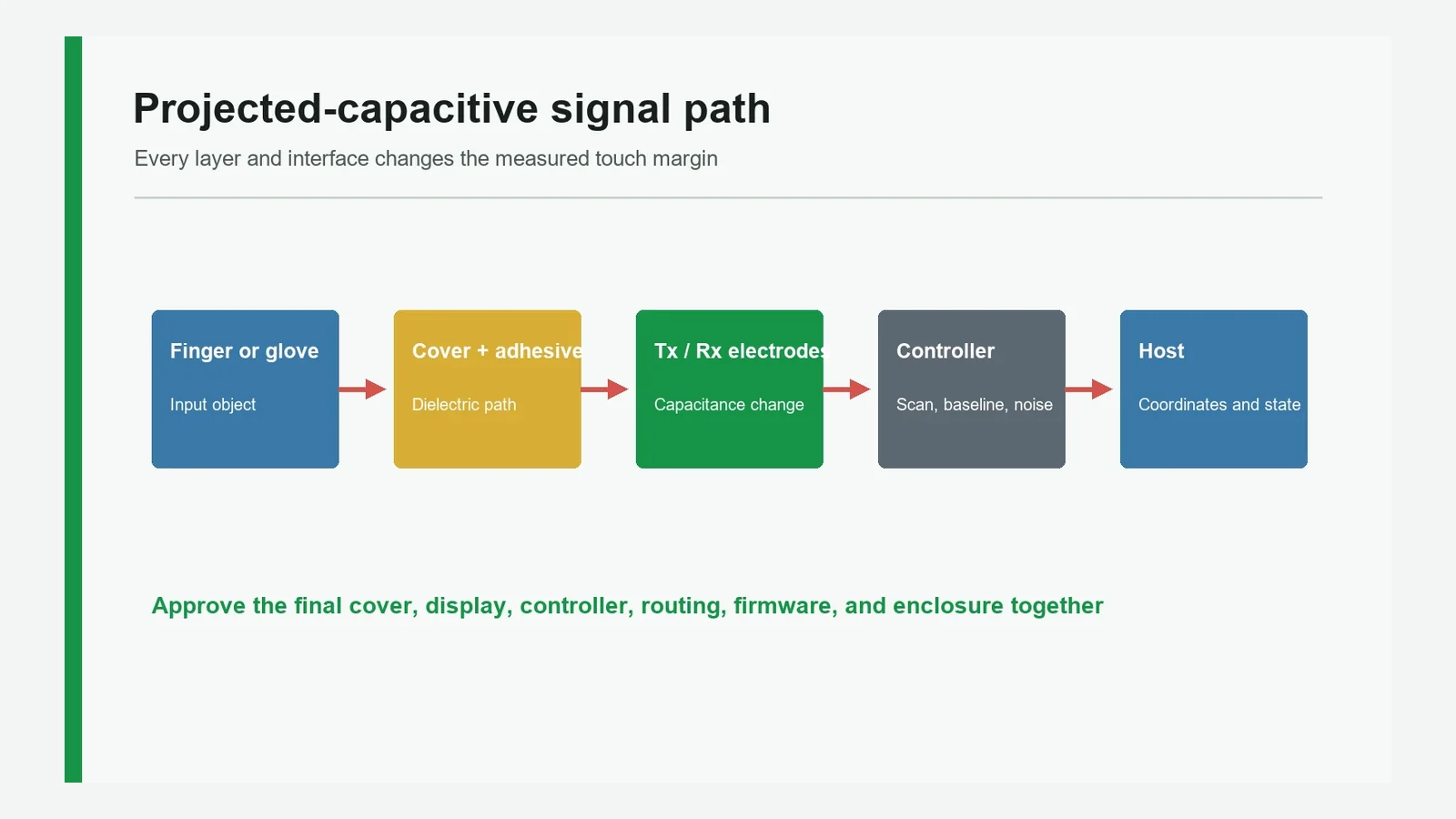
Draw the ESD Current Path From the Accessible Point
An ESD event starts at the cover, seam, screw, bezel, connector, cable shield, or service opening—not at the controller pin. Mark each accessible point, then draw every plausible route to a controlled return.
Possible routes include:
- Blocked by a specified dielectric barrier;
- Redirected into a bonded chassis or perimeter structure;
- Capacitively coupled into an electrode or trace;
- Arced across a seam, edge, opening, or contaminated surface;
- Conducted through a connector and protection network;
- Radiated from the discharge-current loop;
- Returned through circuit ground, cable shield, or protective earth.
IEC 61000-4-2:2025 makes the test reproducible; it does not make a cover lens or loose touch panel independently “ESD rated.” The evidence must identify the complete specimen, mounting, accessible points, operating mode, discharge method, setup, performance criteria, and result.
The cover can be the first barrier, but its dielectric function depends on material, thickness, openings, edge geometry, coatings, adhesive, wear, contamination, and assembly. STMicroelectronics AN3960 describes dielectric overlays, perimeter ground structures, spark-gap concepts, series impedance, protection devices, and firmware recovery as distinct tools. Values shown in that STM32-oriented note are examples under its sensing architecture, not a universal bill of materials.
Protection performance depends on layout. Texas Instruments’ ESD protection guide emphasizes a short source-to-device path, a low-impedance return, minimal stubs, and separation between the high-current region and unprotected circuitry. A TVS placed deep inside a PCB can leave a long trace that radiates and couples before current is diverted.
A touch line adds one more constraint: protection-device capacitance and leakage can reduce sensitivity or distort acquisition. Check operating voltage, clamp behavior, dynamic resistance, capacitance over bias, leakage over temperature, package parasitics, controller limits, and the return destination. Adding a TVS is not the best choice when its loading consumes the required sensor margin or when the real discharge route bypasses it. In that case, insulation, geometry, chassis redirection, connector design, or another controller-approved network may be the correct control.
Treat the Enclosure and Contacts as Electrical Hardware
The enclosure sets field exposure, seam arcs, cable entry, shield termination, part position, and chassis continuity. A cosmetic drawing is not enough.
| Mechanical item | Electrical question | Production evidence |
|---|---|---|
| Metal bezel or frame | Is it floating, circuit-referenced, or chassis-bonded? | Finish callout, contact points, resistance/continuity method |
| Paint, anodizing, plating, or coating | Does the finish preserve or block intended contact? | Masked areas, process control, inspection criterion |
| Gasket and adhesive | Are they conductive, insulating, spacing, or sealing elements? | Material identity, compression/coverage drawing |
| Seams and openings | Can an arc or field reach the flex, PCB, or connector? | Minimum geometry, assembly stack, service condition |
| Fasteners and springs | Do they carry repeatable disturbance current? | Part, torque/contact method, location, change control |
| Cable entry | Where does shield or common-mode current transfer to chassis? | 360-degree or pigtail geometry as designed, not assumed |
A plastic rib that moves the touch flex toward the LCD tail can change noise pickup. Paint under a bonding spring can open the intended ESD return. Conductive tape can reduce display coupling while loading the sensor. Optical bonding can change electrode-to-display spacing. These are electrical changes even when the circuit schematic is untouched.
A Touch Panel EMI ESD Design Test Matrix
Immunity preparation begins with the production-intent stack: cover, sensor, flex, connector, controller, firmware, display, backlight, power system, cables, enclosure, contacts, host software, and representative loads. A sensor coupon is useful for path exploration; it cannot represent the finished HMI.
| Test preparation item | ESD: IEC 61000-4-2 | Radiated RF: IEC 61000-4-3 | EFT/burst: IEC 61000-4-4 | Conducted RF: IEC 61000-4-6 |
|---|---|---|---|---|
| Primary path map | Accessible points, seams, metal, connectors, return | Electrodes, traces, cables, apertures, loops | Power/signal/control/earth ports and shared returns | Coupled cables, shields, reference, person-to-electrode path |
| Operating states | No touch, valid touch, edge/gesture, startup, recovery | All touch modes plus display/backlight/radio states | Load switching, communications, display and host states | Cable, charger, grounded/floating states and valid touch |
| Evidence | Discharge point/method/polarity/time, raw data, reset and damage checks | Frequency/time, orientation, raw channels, host/display logs | Port/coupling/time, burst-correlated events, recovery | Frequency/time, port, channel data, thresholds, host state |
| Acceptance boundary | No unsafe command; declared recovery and damage criteria | No false input; declared missed/latency criteria | No unsafe command or uncontrolled reset | Preserved margin or explicitly controlled inhibition |
| Common mistake | Testing only the flat cover center | Testing one antenna orientation or one display state | Treating a power-port test as proof for signal ports | Using a clean short cable instead of the released harness |
Before formal testing, instrument raw or minimally processed sensor data, baseline, thresholds, touch state, reset reason, configuration, host events, display state, and load state. Synchronize those records with the disturbance. Video alone cannot identify the affected channel. Raw data without the disturbance timestamp cannot identify the entry condition.
EMC and ESD testing must identify the laboratory, equipment, calibration, method edition, specimen count, setup, report format, and responsibility split. The applicable IEC level and acceptance limits come from the finished-equipment requirements and the approved test plan.
Use progressive evidence:
- Path exploration: sensor, controller, source, and controlled coupling setup.
- Powered front stack: production-intent cover, sensor, flex, display, controller, and supply.
- Enclosure prototype: released mounting, seams, contacts, cables, shield, and gasket.
- Integrated equipment: representative loads, software, harnesses, and operating states.
- Formal article: controlled build tied to drawings, BOM, firmware, enclosure, cables, and test plan.
Change one variable at a time during diagnosis. If firmware, shield, filter, enclosure bond, and flex route all change together, a passing sample does not reveal which controls are necessary.
Diagnose Failures by Frequency, Location, Cable, and State
A reproducible signature narrows the first interfaces to inspect.
| Observation | First interfaces to investigate |
|---|---|
| One electrode group fails in a narrow frequency band | Local route, LCD tail, scan frequency, shield coverage, connector pins |
| All channels move together | Supply/reference, cable-borne common mode, charger, chassis bond |
| Failure follows image or brightness | Display interface, frame, backlight converter, shared return, flex overlap |
| ESD at one seam resets the controller | Seam arc, chassis contact, protection return, reset/supply path |
| Air discharge fails but contact to exposed metal does not | Edge insulation, opening, contamination, arc path, field coupling |
| Contact discharge damages one channel | Entry trace, protector placement, return, connector, controller pin |
| Open bench stack passes but closed enclosure fails | Flex movement, bezel loading, paint/contact, cable loop, gasket pressure |
| Filtering removes false touches but causes missed input | Threshold, latency, scan rate, valid-touch margin, state logic |
| Failure changes with cable orientation | Conducted current, cable loop, shield termination, chassis reference |
Repeat the smallest failing condition before accepting a correction. Then alter the suspected path and repeat the same stimulus, setup, operating state, and evidence capture. Preserve both records.
Do not diagnose from the visible screen alone. A host communication fault can look like a frozen touch controller. A controller reset can look like a missed touch. Display corruption can hide a correct touch event. Separate sensor, controller, host, display, and machine logs.
Prepare the Electrical and Enclosure Constraints
A useful supplier review starts with a controlled input package, not a request for an “EMI-proof panel.” Include:
- cover material, nominal stack, printed regions, openings, edges, and adhesive;
- electrode construction, trace map, flex stack, connector, exposed-contact side, and bend state;
- selected controller, acquisition method, approved external components, and raw-data access;
- LCD model/revision, frame, display tail, interface, image modes, and backlight converter;
- power tree, adapter/charger, grounding state, switching sources, loads, and external cables;
- controller reference, power return, display frame, chassis, shield, guard, cable shield, protective earth, and ESD return;
- enclosure material, finish, seams, contacts, fasteners, gasket, cable exits, and service openings;
- required no-touch, valid-touch, glove/wet, startup, sleep, wake, and fault states;
- product-standard requirements, IEC method editions, severity, setup, and performance criteria;
- released BOM, firmware/configuration identifiers, approved alternates, and revalidation triggers.
JASPER’s capacitive-touch HMI assemblies offer a related route for discussing the physical panel, display, electronics, cables, and enclosure as an integration package. Availability of specific controller tuning, protection design, EMC instrumentation, laboratory testing, or compliance responsibility must be confirmed in writing for the actual project.
The next step is to review the electrical and enclosure constraints against the source-path ledger. Assign every open item to the OEM, touch-panel supplier, controller vendor, display supplier, enclosure supplier, firmware owner, or test laboratory. The deliverable is not a blanket immunity promise. It is a controlled specimen, explicit acceptance criteria, traceable failure paths, and evidence that remains valid when the product changes.
Frequently Asked Questions
What is the difference between EMI and ESD in a capacitive touch panel?
EMI is the broader disturbance problem, including radiated fields, cable-coupled RF, switching noise, and burst. ESD is a short, high-energy discharge event addressed by IEC 61000-4-2. Their entry paths and corrections differ, so an ESD result cannot prove general noise immunity.
Should a capacitive touch shield connect to circuit ground or chassis?
There is no universal answer. The correct reference depends on whether the structure is a passive shield, controller-driven shield, cable shield, display frame, or chassis element. Its coverage, current path, termination impedance, controller loading, and production continuity must be defined before choosing the connection.
Can firmware fix capacitive touch noise immunity problems?
Firmware can filter, change sensing frequency, reject improbable patterns, inhibit input, recover, and log faults. It cannot correct a long ESD return, uncontrolled common-impedance current, poor flex placement, or an arcing enclosure seam. Hardware containment and firmware behavior need separate evidence.
Why does an LCD or backlight cause false touches?
LCD timing, display cables, frame potential, and backlight conversion can couple into electrodes, sensor traces, or the controller reference. Test representative image transitions, refresh modes, brightness states, startup, and sleep—not only one static screen—to identify the display-dependent path.
Why can a charger make a capacitive touch panel unstable?
A charger can add common-mode and differential noise through its output cable and grounding capacitance. When a user touches the sensor, the person’s coupling to earth can complete a noise path into the electrode. Test the released adapter, cable, load, and grounded or floating state.
Does adding a TVS diode guarantee ESD protection?
No. A TVS must intercept the actual entry path and return current through a short, low-impedance route. Its capacitance and leakage must also preserve touch margin. If current bypasses the device or the device overloads the sensing node, another geometry or protection strategy is required.
Which IEC 61000-4 tests are relevant to a touch-panel HMI?
Common basic methods include IEC 61000-4-2 for ESD, -4-3 for radiated RF, -4-4 for EFT/burst, and -4-6 for conducted RF. The governing product standard determines applicability, severity, setup, operating mode, and performance criteria for the finished equipment.
Must the complete HMI assembly be retested after a display or enclosure change?
At minimum, the affected paths require documented revalidation. A display, FPC, bezel, coating, gasket, cable, shield termination, or enclosure contact can change sensor loading and disturbance current. The project change matrix should decide whether targeted checks or the full formal sequence must be repeated.
Technical References
- Source: Texas Instruments TIDM-CAPTOUCHEMCREF Design Guide. Accessed 2026.
- Source: IEC 61000-4-2 Electrostatic Discharge Immunity. Accessed 2026.
- Source: IEC 61000-4-3 Radiated RF Immunity. Accessed 2026.
- Source: IEC 61000-4-4 Electrical Fast Transient Immunity. Accessed 2026.
- Source: IEC 61000-4-6 Conducted RF Immunity. Accessed 2026.
- Source: Renesas Capacitive Touch Noise Immunity Guide. Accessed 2026.
- Source: onsemi TND6033 Touch Screen EMI and ESD Protection. Accessed 2026.
- Source: Microchip AN2934 Capacitive Touch Sensor Design Guide. Accessed 2026.
- Source: Infineon AN85951 CAPSENSE Design Guide. Accessed 2026.
- Source: STMicroelectronics AN3960 ESD for Touch Sensing Applications. Accessed 2026.
- Source: Texas Instruments ESD Protection Layout Guide. Accessed 2026.
- Source: Analog Devices AN-957 CapTouch Controller Layout Guide. Accessed 2026.
- Source: Texas Instruments, “TIDM-CAPTOUCHEMCREF Noise-Tolerant Capacitive-Touch HMI Reference Design” and design guide. Accessed 2026.
- Source: International Electrotechnical Commission, “IEC 61000-4-2:2025 — Electrostatic discharge immunity test.”. Accessed 2026.
- Source: International Electrotechnical Commission, “IEC 61000-4-3:2020 — Radiated, radio-frequency, electromagnetic field immunity test.”. Accessed 2026.
- Source: International Electrotechnical Commission, “IEC 61000-4-4:2012 — Electrical fast transient/burst immunity test.”. Accessed 2026.
- Source: International Electrotechnical Commission, “IEC 61000-4-6:2023 — Immunity to conducted disturbances induced by radio-frequency fields.”. Accessed 2026.
- Source: Renesas Electronics, “Capacitive Touch Noise Immunity Guide,” R30AN0426EJ0400, Rev. 4.00, December 27, 2024. Accessed 2026.
- Source: onsemi, “TND6033/D Touch Screen EMI/ESD Protection,” Rev. 1, February 2014. Accessed 2026.
- Source: Microchip Technology, “AN2934 Capacitive Touch Sensor Design Guide,” DS00002934B. Accessed 2026.
- Source: Infineon Technologies, “AN85951 PSoC 4 and PSoC 6 MCU CAPSENSE Design Guide,” Rev. AI, May 26, 2026. Accessed 2026.
- Source: Infineon Technologies, “AN234185 PSoC 4 CAPSENSE Touchpad Design Guide.”. Accessed 2026.
- Source: Microchip Technology, “MXTAN0208 Design Guidelines for PCB Layouts for maXTouch Controllers.”. Accessed 2026.
- Source: STMicroelectronics, “AN3960 Guidelines for ESD for Touch Sensing Applications on STM32 MCUs,” Rev. 8, February 27, 2025. Accessed 2026.
- Source: Texas Instruments, “ESD Protection Layout Guide,” SLVA680B. Accessed 2026.
- Source: Analog Devices, “AN-957 Layout Guidelines for AD7147/AD7148 CapTouch Controllers.”. Accessed 2026.
Review the complete interference and discharge path
Send the sensor and display stack, flex route, grounding, enclosure contacts, power states, protection network, firmware behavior, and test plan.