
A sound silicone keypad HMI assembly design treats the keypad, conductive contacts, PCB, bezel, and enclosure as one tolerance-controlled mechanism. OEM mechanical, electrical, quality, and manufacturing engineers must set compression from the selected elastomer and hard-stop geometry, then prove contact overlap and key motion at stack limits. There is no universal compression percentage or PCB-pad allowance. Controller software and finished-equipment approval remain outside this mechanical release decision.
1. Define the Assembly Before Setting Compression
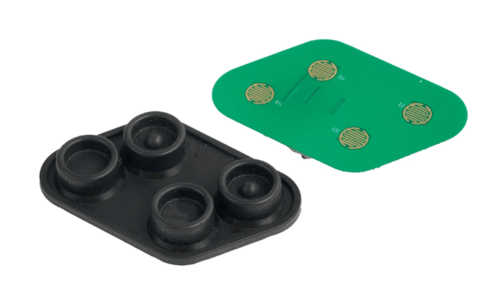
A rubber keypad HMI is a mechanism, not just a molded sheet over a circuit board. Finger load passes through a key and web to a conductive contact, PCB, and local support. The flange, bezel, bosses, and fasteners locate and close the stack.
Write that physical boundary before selecting compression. JASPER's silicone keypad HMI assemblies page is the relevant commercial route, but the BOM decides what is supplied. The HMI assembly overview separates a physical module from its controller, firmware, and finished machine.
| Boundary | Typical controlled content | What the boundary does not prove |
|---|---|---|
| Molded keypad | Key tops, web geometry, flange, locating features, legends/coatings if specified, conductive pills if specified | Installed compression, PCB alignment, enclosure fit, or finished-equipment protection |
| Keypad–PCB subassembly | Molded keypad, PCB contact pattern, local support, connector, hardware listed in the BOM | Bezel clearance, enclosure hard stops, service access, or final ingress performance |
| Complete physical HMI module | Released keypad, PCB, bezel/carrier, gasket, fasteners, connector route, labels, and agreed checks | Host software, safety logic, cabinet wiring, or automatic regulatory approval |
| Finished equipment | HMI module plus enclosure, controller, software, power, wiring, and application controls | Nothing beyond the conformity and validation scope actually declared by the OEM |
A loose keypad can meet its drawing while a tall boss bends the PCB, a shifted bezel rubs a key skirt, or fastener clearance lets the pill miss the usable pad. These interface failures cannot be prevented until the release names the full stack.
2. Read the Stack as Two Coupled Load Paths
A silicone keypad assembly carries two different loads. The actuation path runs from the user's finger through the key and conductive contact into the PCB support. The retention or sealing path runs from the bezel or enclosure through the keypad flange, gasket features, hard stops, bosses, and fasteners. The paths interact, but they should not be confused.
Conceptual stack—operator side to equipment side:
OPERATOR
actuation load Key top / legend / coating Web or flexure · must move without bezel or wall interference Conductive pill · follows a controlled trajectory PCB contact pattern · minimum usable overlap at worst-case offset PCB support land · reacts key load without excessive local deflection
RETENTION / SEALING PATH Bezel face and key openings Molded flange / seal bead / locating features Hard-stop gap · sets installed thickness; fastener torque closes to it Bosses, ribs, carrier, and enclosure Fasteners / latches · clamp the structure; not a substitute for a gap datum
FINISHED-EQUIPMENT ENCLOSURE
This is a design map, not a universal recipe. Some silicone keypad assemblies use a rigid PCB; others use a membrane or flexible circuit, light guide, or carrier. A flange may retain without sealing, while a seal bead may need a load path separate from the key web.
HMI keypad compression is an installed-gap result
If the free molded flange thickness is (t_f) and the closed hard-stop gap is (g), geometric flange compression is:
[ C_f(%) = 100\left(1-\frac{g}{t_f}\right) ]
The equation is simple; the permissible window is not. It depends on thickness distribution, flange geometry, elastomer formulation, temperature history, load-deflection behavior, sealing objective, and retained deformation. ASTM D395-18(2024) provides compression-set methods; ASTM D575-91(2018) addresses rubber in compression. Neither prescribes one keypad percentage.
A hard stop should establish the closed gap. Torque still secures the joint, but thread friction, surface condition, housing stiffness, and tightening sequence make it a weak geometric control. When sealing and key motion share uncontrolled squeeze, tightening the case can alter feel or prevent a contact from opening.
Contact alignment is an overlap problem, not a centerline promise
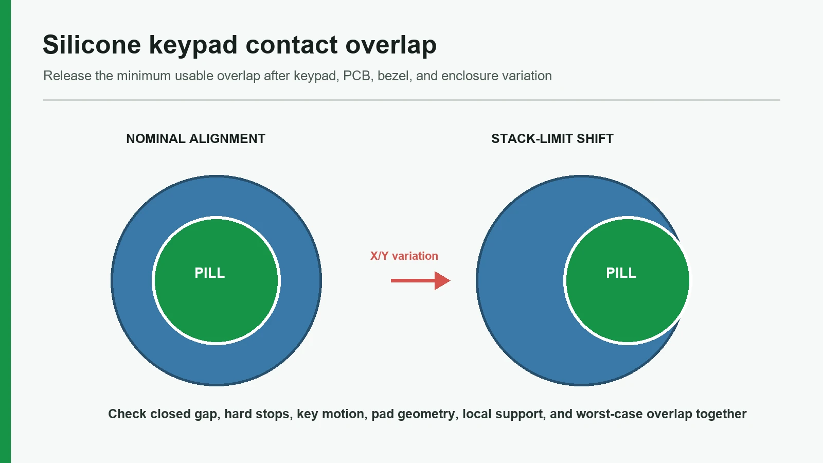
Nominal concentricity can fail at tolerance limits. Define the usable PCB region, the pill's landing region, and the minimum overlap left after keypad molding, locator clearance, PCB fabrication/location, enclosure tooling, fastener float, and assembly shift.
For a signed one-dimensional relationship (y=\sum a_i x_i), a conservative worst-case screen is:
[ T_{WC}=\sum |a_i|T_i ]
why root-sum-square treatment needs justified variation and covariance assumptions. Use worst case for a hard overlap or interference boundary until stable measured distributions justify another method. Acceptable overlap remains project-specific to the pill, pad, travel, finish, mask, contamination control, and electrical evidence.
3. What Fails When the Stack Is Released by Nominal CAD
Nominal CAD shows perfect parts. Production must show how allowed parts move, compress, bow, and interfere. A keypad, PCB, and enclosure can each pass inspection while the assembly gives intermittent keys or uneven feel.
| Release error | Physical mechanism | User or test symptom | Controlling evidence |
|---|---|---|---|
| Flange squeezed without a hard-stop window | Clamp load changes molded thickness and can distort nearby webs | High or uneven force; key remains partly depressed; feel changes after assembly | Min/max installed-gap calculation plus production-intent force–displacement data |
| Bezel opening checked only at nominal position | Key skirt or web enters the moving envelope of the bezel | Scrape, slow return, off-axis feel, cosmetic rub mark | Displaced-geometry clearance check at full travel and tolerance limits |
| Pill and pad dimensioned from unrelated origins | Locator and fabrication offsets consume contact overlap | Intermittent closure, higher resistance, edge wear, sensitivity to side load | Shared datum frame and minimum-overlap requirement |
| PCB spans between distant supports | Actuation bends the board instead of closing the contact predictably | Soft feel, double actuation, force variation by key location | Local support map and assembled force/closure measurement |
| Boss height competes with flange gap | One feature bottoms before the intended hard stops | PCB bow, case gap, local over-compression, fastener loosening | Complete vertical stack and sectioned min/max analysis |
| Solder mask, residue, or finish is unspecified at contacts | Usable conductive area or surface condition varies | Missed, unstable, or drifting contact closure | Released contact land, finish, mask keep-out, cleanliness and electrical acceptance |
| Assembly has rotational symmetry with no poka-yoke | Keypad or PCB can be installed in a wrong orientation | Wrong key map, shifted contacts, pinched tail | Keyed locators, clear work instruction, post-assembly functional test |
| Service screws are tightened in an uncontrolled sequence | Flexible bezel or enclosure closes unevenly | Keys pass at factory but fail after service | Torque/sequence instruction, reusable hard stops, reassembly verification |
Hardness is another shortcut. ASTM D2240-15(2021) controls durometer measurement, but Shore A does not determine key feel. Web geometry, travel, preload, key mass, off-axis load, coating, temperature, contact, and support all contribute. Approve the assembled force–displacement curve.
4. A 10-Point Silicone Keypad HMI Assembly Design Framework
This framework turns the stack into ten release decisions: scope, datums, compression, motion, contact, PCB construction, support, tolerance, service, and approval. Each criterion has an auditable signal and a stop-release warning.
4.1 Freeze the supply and validation boundary
The validation boundary follows. IEC 60529 classifies enclosure protection; it does not make a loose silicone mat IP-rated. IEC 60601-1 concerns medical electrical equipment and systems, not automatic component approval.
every BOM line has a sourcing owner, revision, included/reference status, and inspection state.
the quotation, CAD assembly, electrical drawing, and test plan show different scopes.
4.2 Put keys, pills, pads, and openings on one functional datum frame
Choose datums that survive assembly: a mounting face for the vertical stack, then tooling holes, posts, or an edge for planar position and rotation. Key centers, pills, PCB pads, bezel openings, legends, and enclosure locators should resolve to this frame.
ASME Y14.5-2018 (R2024) and ISO 5459:2024 provide datum systems but do not choose these HMI datums. Identify the governing drawing convention and select features that represent function.
a reviewer can trace each critical relationship to the same datum reference frame across the keypad, PCB, and enclosure drawings.
overlay artwork, molded tools, PCB Gerbers, and mechanical CAD use different zero points with undocumented translations.
4.3 Set flange compression from a closed-gap window
Define the free feature, the surfaces creating the gap, and all min/max contributors. Retention or sealing may drive the lower limit; closure load, permanent deformation, web distortion, housing stress, or poor return may drive the upper limit.
State free thickness, gap limits, hard stops, flash zones, and surfaces excluded from clamp load. Measure closing force and function at both limits. Compression-set evidence under relevant time and temperature differs from immediate load; ASTM D395 offers a method, not an automatic pass.
min/max gap analysis and selected-material evidence define a project compression window, with hard stops outside moving webs.
a generic percentage is copied from a blog and applied to a different elastomer, flange profile, or sealing function.
4.4 Keep bezel support outside the moving key envelope
The opening must clear the keycap, skirt, and displaced web through full travel at size and position limits. A top-plane gap misses lateral web bow and tilted off-axis actuation. Model the moving envelope or inspect sectioned samples at worst offset.
Support the flange or dedicated seats, never the flexible web. A nearby land can stiffen one side. A guide wall becomes a friction interface requiring controlled clearance and finish.
drawings show the moving envelope, minimum side clearance, support zones, and no-contact zones at full travel.
the only check is a nominal top-view gap between the keycap and bezel opening.
4.5 Release silicone keypad PCB alignment as minimum contact overlap
Identify each pill's shape and landing trajectory. Define the usable PCB area after mask, edge chamfer, vias, and contamination keep-outs. Require overlap at worst relative offset—not just nominal center position.
Include pill-to-keypad locator, locator-to-enclosure, pad-to-PCB tooling, PCB-to-enclosure, and assembly float. Analyze X, Y, and rotation; rotation grows more important with distance from the locator origin.
the assembly drawing or interface-control document states a verified minimum overlap under a named datum scheme and tolerance method.
the PCB pad was enlarged until nominal CAD looked comfortable, without checking mask, nearby conductors, or worst-case rotational shift.
4.6 Specify the PCB contact zone as an electrical and mechanical interface
Distinguish keypad contacts from ordinary component pads. Control geometry, copper definition, finish, solder-mask opening, vias, cleanliness, flatness/support, and protective processing. State whether the pill bridges interdigitated lands, concentric features, or another pattern.
IPC-2221B gives generic board-design principles; IPC-2222B covers rigid organic boards. IPC-6012E, when invoked, can control rigid-board qualification/performance. None proves that a selected conductive-rubber contact works on the finished pad.
the released PCB package names the entire contact construction and preserves test access without placing unsupported features beneath the key.
“PCB per IPC” is the only contact specification.
4.7 Place local support beneath the actuation path
If the PCB flexes, key travel is lost to board deflection and feel varies by location. Map each load to a boss, rib, carrier, or backplate. Keep supports clear of solder joints, vias, components, lights, and contact regions.
Supports must not compete with flange hard stops. At tolerance limits, an equal-height boss can bottom first and bow the PCB. Section drawings should show the intended order of contact.
each key has an intentional load path to a controlled support, and min/max sections show the designed order of contact.
the PCB is treated as a rigid plane despite long spans, edge fasteners, or uneven component clearances.
4.8 Budget the full enclosure tolerance stack
Keep one stack model covering keypad features, pill location, PCB tooling/pads, bosses/locators, bezel opening, enclosure flatness, fastener clearance, fixture repeatability, and positional adhesive or gasket layers.
Worst case tests interference and minimum overlap. A statistical model needs stable processes, distributions, and correlations. NIST's capability guidance compares a stable process with specification limits; it cannot repair an undefined limit.
the stack names every contributor, sign, datum, source drawing, limit, and verification owner.
nominal assembly clearance is called “tolerance” or an RSS result is used without measured distribution evidence.
4.8.1 Release evidence for the installed stack
| Controlled relationship | Required project input | Approval evidence |
|---|---|---|
| Keypad flange to hard stop | Molded thickness, closed gap, material and tolerance | Measured compression window on production-intent parts |
| Conductive pill to PCB pad | Pill contact area, pad geometry and full X/Y stack | Minimum usable overlap at every tolerance limit |
| Key web to bezel opening | Key motion envelope, bezel opening and assembly shift | Off-axis actuation and return without rubbing |
| PCB to local support | Board thickness, support position and fastener state | Closure, force-displacement and contact stability records |
| Service reassembly | Locator, torque or hard-stop method and replacement parts | Repeatable fit and function after the released service cycle |
4.9 Design service assembly so it returns to the same state
A factory fixture can hide poor service design. Without it, a person may alter fastener order, pinch a tail, roll the flange, or rotate a symmetric part. Use keyed geometry, orientation marks, captured features, and a sequence that avoids manual centering.
Specify reusable parts, tightening pattern, hard-stop inspection, connector handling, and post-service checks. If opening disturbs a seal, define replacement and any repeated enclosure test; uncontrolled reassembly cannot inherit the original IEC 60529 result.
a trained person can disassemble and rebuild the unit with production-intent tools, then reproduce gap, key function, and inspection results.
service success depends on “careful alignment” with no locators, fixture, or measurable acceptance point.
4.10 Approve the production-intent stack, not a collection of loose parts
Approve dimensional relationships and motion on representative parts, then measure assembled force–displacement, closure, return, and off-axis behavior. Repeat after relevant conditioning. IEC 60068-2-6, IEC 60068-2-27, IEC 60068-2-14, and IEC 60068-2-78 offer vibration, shock, temperature-change, and damp-heat methods; the OEM owns severities and limits.
For road vehicles, ISO 16750-1:2023 links environmental loads to mounting location and application. The program must still define parts, profiles, powered state, monitoring, samples, and failure criteria.
one approval plan ties each failure mode to a production-intent specimen, condition, measurement, limit, and decision owner.
molded dimensions, PCB continuity, and enclosure fit pass separately, but no assembled contact/return evidence exists.
5. Run the Release Process in Six Steps
A six-step process closes interfaces before tooling and preserves them through change control.
Step 1 — Collect native inputs and define ownership
Gather keypad CAD/drawing, PCB data and outline, enclosure CAD, key map, circuit matrix, connector, target feel, environment, cosmetic zones, service concept, and standards. Mark ownership and record revisions.
Step 2 — Build the shared datum and load-path model
Select assembly datums. Trace each key through web, pill, pad, PCB, support, stop, and enclosure. Mark moving envelopes, compression zones, no-load zones, and possible early contacts. Reconcile coordinate systems before release.
Step 3 — Calculate compression, clearance, and contact overlap
Build vertical and planar stacks. Identify free elastomer thickness, closed gaps, boss heights, PCB contributors, and first-contact surfaces. Calculate pill/pad overlap and key/opening clearance through translation and rotation. Use RSS only after process distributions are demonstrated.
Step 4 — Build production-intent prototypes
Use representative molded geometry, PCB contacts, enclosure process, locators, supports, stops, and fasteners. A 3D-printed housing can answer fit questions but misrepresent stiffness, surface, warpage, and fastening. Label every nonrepresentative property.
Step 5 — Approve functions and limits together
Measure gaps, return, force–displacement, closure, electrical stability, registration, edge keys, and off-axis actuation. Repeat after relevant conditioning. JASPER's testing and validation planning uses a failure-mode structure but does not prove any project passed.
Step 6 — Release production controls and change rules
Release incoming checks, fixture references, sequence, fastener controls, functional test, visual criteria, traceability, and reaction plan. Review changes to silicone, mold, pill, PCB finish/mask or fabricator, enclosure tool, bosses, locators, fastener, gasket, adhesive, or assembly site.
The anonymized HMI front-panel assembly case illustrates coordination of controls, PCB, fasteners, cables, and housing datums. It is not a customer or performance claim for this design.
6. Drawing and Project-Input Checklist
The package should let a reviewer reconstruct the stack without guessing.
Keypad definition
- [ ] Native 3D model plus controlled 2D drawing and revision
- [ ] Key centers, key map, travel direction, web/no-contact zones, and moving envelopes
- [ ] Free-state flange and seal geometry with thickness limits
- [ ] Locators, allowable flash/parting-line zones, coating/legend scope, and orientation feature
- [ ] Conductive-pill geometry, position, material system, and approved electrical acceptance method
- [ ] Target assembled force–displacement and return criteria—not hardness alone
PCB definition
- [ ] Mechanical outline, tooling/locator features, thickness, and critical flatness/support requirements
- [ ] Contact-pad geometry, usable area, copper definition, finish, solder-mask keep-out, and via restrictions
- [ ] Key matrix/netlist, connector/pinout, test points, component and routing keep-outs
- [ ] Fabrication/acceptance standard when required, plus project-specific contact criteria
Bezel and enclosure definition
- [ ] Native CAD, material/process, mounting face, datum system, and drawing revision
- [ ] Key openings, walls, support lands, hard stops, boss/rib map, fasteners, and tightening sequence
- [ ] Min/max closed gaps, allowed warpage/flatness contributors, and sealing boundary
- [ ] Service access, connector route, cable/tail protection, and replacement instructions
Approval definition
- [ ] Complete tolerance stack and minimum pill-to-pad overlap requirement
- [ ] Prototype representativeness statement and sample configuration
- [ ] Test matrix with environment, mounting, powered state, measurements, limits, and owner
- [ ] Golden sample or approved references where appropriate
- [ ] Production inspection, functional test, change notification, and revalidation triggers
The CTA is concrete: share the keypad, PCB, and bezel stack together, including enclosure stops and locators. A keypad drawing alone cannot close HMI keypad compression or contact registration.
7. Prototype and Approval Test Matrix
A test needs a specimen, setup, condition, output, and acceptance owner. Populate this planning matrix from the product requirement and selected materials.
| Stage / failure mode | Production-intent specimen and setup | Measure before / during / after | Acceptance must define | Evidence owner |
|---|---|---|---|---|
| Dimensional stack | Keypad, PCB, bezel/enclosure, hard stops, supports, and actual fastening method | Free thickness, closed gaps, key-to-opening clearance, pill/pad registration, PCB support contact | Min/max dimensions and no-interference/minimum-overlap rules | Mechanical design + supplier quality |
| Force and return | Complete stack at controlled temperature, using stated actuator size/location/rate | Force–displacement curve, contact point, return, hysteresis, off-axis behavior | Key-specific windows and repeatability method | HMI/mechanical design |
| Electrical closure | Released contact construction, circuit, scan/load condition, and fixture | Closure state, resistance or voltage criterion if required, bounce/debounce observation, open return | Circuit-specific pass limits and measurement method | Electrical design |
| Assembly variation | Stack-limit parts or justified fixtures representing min/max gaps and offsets | Function across translation, rotation, boss/gap, and fastener conditions | Every allowed build meets clearance, overlap, closure, and return boundaries | Design authority |
| Retained compression | Selected elastomer/specimen and assembled stack under defined time/temperature | Compression set or dimensional recovery, closing load, post-condition key function | Material and assembly limits tied to actual use | Materials + reliability |
| Temperature / damp heat | Complete module in defined powered/unpowered state | Gaps, force/return, closure, visual changes, seal/interface condition | Severity, dwell, recovery, monitoring, and functional limits | Reliability / OEM |
| Vibration / shock if applicable | Module mounted with production bracket, fasteners, cable, and orientation | Intermittent contacts during test if required; function and inspection afterward | Profile, axes, monitoring bandwidth, anomalies, post-test limits | System reliability |
| Service reassembly | Trained assembler using released instructions and intended tools | Orientation, pinching, gap/torque sequence, function, seal replacement state | Repeatable rebuild and required post-service checks | Service engineering + quality |
| Production control | Production fixture and end-of-line electrical/mechanical checks | Critical dimensions or go/no-go state, all-key function, connector/pinout, visual defects | Sampling/100% test rule, limits, reaction plan, traceability | Manufacturing quality |
Do not derive cycle life from a material or loose keypad when risk lies in the stack. ASTM F1578-24 covers membrane-switch contact cycling; apply it only when the contact and specification fit its scope. Define cycle count, actuator, electrical load, environment, monitoring, and failure.
8. When a Rubber Keypad HMI Is Not the Best Choice
A silicone keypad is not always the right interface. Consider another construction when the interaction or environment conflicts with its mechanism.
| Project condition | Construction worth evaluating instead | Why |
|---|---|---|
| Dense changing labels, gestures, maps, or rich visual feedback dominate | Touchscreen or display-centered HMI with separate critical controls | A fixed molded key field cannot change its information architecture |
| The operator needs continuous rotational input or fine incremental adjustment | Encoder, joystick, or dedicated electromechanical control | Discrete elastomer keys do not provide the same motion model or resolution |
| The enclosure cannot provide reliable hard stops or local PCB support | Self-contained switch modules or a separately supported keypad carrier | The proposed stack lacks a stable reaction and compression path |
| Very small pitch leaves inadequate web, bezel, and contact tolerances | Dome/membrane switch, capacitive keys, or another compact input technology | The tolerance budget may consume usable movement and contact overlap |
| A safety function requires independent architecture and diagnosed states | Application-specific safety-rated controls | A standard rubber keypad contact is not a safety function by declaration |
| Field contamination or cleaning cannot be validated at the assembled enclosure | A construction selected and tested specifically for that exposure | Silicone alone does not establish chemical resistance or an enclosure IP code |
Choose from the operator task and equipment risk analysis. A rubber keypad HMI fits tactile discrete inputs, shaped keys, integral graphics, and a compact stack when service and validation support it.
9. Frequently Asked Questions
What controls silicone keypad HMI assembly design?
The full load path and tolerance chain control the design: key/web motion, pill trajectory, PCB contact, board support, flange compression, bezel openings, stops, locators, and assembly variation. No single property or component drawing controls it.
What percentage should a silicone keypad flange be compressed?
No universal percentage is defensible. Calculate from free flange thickness and min/max hard-stop gap, then set limits from the elastomer, geometry, load-deflection/compression-set evidence, seal objective, and assembled tests. ASTM D395 supports testing, not selection of the percentage.
How is silicone keypad PCB alignment toleranced?
Tolerance the minimum overlap between pill landing and usable PCB contact. Use a common datum frame, include molding, PCB, enclosure, locator, fastener, assembly, and rotation contributors, then verify overlap at worst offset.
Does Shore A hardness determine keypad feel?
No. ASTM D2240 measures Shore A hardness, but feel also depends on web geometry, travel, preload, key size, contact motion, off-axis load, coating, temperature, bezel clearance, PCB deflection, and support. Approve assembled force–displacement and return.
Should the bezel or PCB set the installed keypad height?
Dedicated enclosure or carrier stops should set the gap. A PCB may participate only when its support and thickness are controlled in the stack. Flexible bezels, unsupported boards, or torque alone should not set height.
What PCB details matter for conductive-rubber contacts?
Control pad shape and usable area, copper, finish, solder mask, vias, cleanliness, flatness, support, locator relationship, and test state. IPC board acceptance can govern fabrication but does not prove assembled conductive-pill closure.
How should service reassembly be validated?
Run a controlled rebuild with released instructions, tools, orientation controls, fastener sequence, replacement parts, and post-service checks. Confirm restored gap, motion, contacts, cable route, and any enclosure retest required after disturbing a seal.
When is a rubber keypad HMI not the best interface?
Avoid it when the interface needs changing labels and gestures, continuous rotary control, very fine pitch without tolerance margin, no stable support/stop path, or a safety-rated architecture. Compare touchscreen, encoder, membrane/dome, switch-module, and safety-control options.
10. Next Step: Review the Stack, Not the Keypad Alone
Before tooling, combine the keypad CAD/drawing, PCB contacts, enclosure CAD, hard-stop sections, locators, key map, and tests in one controlled package. This exposes excess squeeze, web interference, weak overlap, unsupported PCB spans, competing bosses, and service errors.
JASPER is one option for reviewing silicone keypad HMI assemblies. Ask for a review of the keypad, PCB, bezel, and enclosure stack against required feel, contacts, service, and validation—not a loose keypad review. The quotation, BOM/drawings, and testing and validation plan should state JASPER's scope and the evidence retained by the OEM.
Technical References
- Source: ASTM D395-18(2024). Accessed 2026.
- Source: ASTM D575-91(2018). Accessed 2026.
- Source: NIST's propagation guidance. Accessed 2026.
- Source: ASTM D2240-15(2021). Accessed 2026.
- Source: IEC 60529. Accessed 2026.
- Source: IEC 60601-1. Accessed 2026.
- Source: ASME Y14.5-2018 (R2024). Accessed 2026.
- Source: ISO 5459:2024. Accessed 2026.
- Source: ASTM D395. Accessed 2026.
- Source: IPC-2221B. Accessed 2026.
- Source: IPC-2222B. Accessed 2026.
- Source: IPC-6012E. Accessed 2026.
- Source: NIST's capability guidance. Accessed 2026.
- Source: IEC 60068-2-6. Accessed 2026.
- Source: IEC 60068-2-27. Accessed 2026.
- Source: IEC 60068-2-14. Accessed 2026.
- Source: IEC 60068-2-78. Accessed 2026.
- Source: ISO 16750-1:2023. Accessed 2026.
- Source: ASTM F1578-24. Accessed 2026.
- Source: ASTM D395-18(2024): Rubber Property—Compression Set. Accessed 2026.
- Source: ASTM D2240-15(2021): Rubber Property—Durometer Hardness. Accessed 2026.
- Source: ASTM D575-91(2018): Rubber Properties in Compression. Accessed 2026.
- Source: ASTM F1578-24: Contact Closure Cycling of a Membrane Switch. Accessed 2026.
- Source: IPC-2221B generic printed-board design scope. Accessed 2026.
- Source: IPC-2222B rigid-board design scope. Accessed 2026.
- Source: IPC-6012E rigid-board qualification/performance scope. Accessed 2026.
- Source: Y14.5-2018 (R2024), Dimensioning and Tolerancing. Accessed 2026.
- Source: ISO 5459:2024, Geometrical tolerancing—Datums and datum systems. Accessed 2026.
Review the complete HMI assembly before design release
Send the front-panel drawing, stack, display, circuit, connector, enclosure, service conditions, and acceptance plan for review.