
A sound capacitive HMI front panel design releases the cover lens, printed mask, touch sensor, bond lines, display, bezel, controller PCB, grounding, connector, and enclosure datums as one controlled system. This guide helps OEM mechanical, electronics, display, quality, and sourcing teams decide that stack before tooling. It establishes what purchasing must specify and what validation must prove. It does not prescribe universal layer thicknesses or prove IP/EMC compliance; controller tuning and final validation must use production-intent hardware in the finished enclosure.
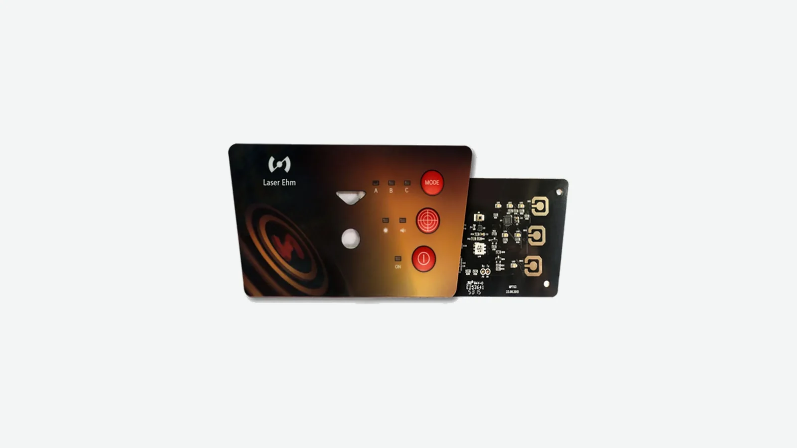
Why Capacitive Front Panels Fail at Layer Interfaces
A capacitive front panel assembly rarely fails because the project forgot a cover lens or touch controller. Trouble starts at an interface: the display shifts relative to the black mask; an adhesive keep-out leaves a local air gap; a ground pour loads the electrode; a metal bezel couples noise into the sensor; or the tail bends across a stiffener edge. Each part can pass incoming inspection while the assembled HMI still misses touches, shows bubbles, leaks light, or resets during electrostatic discharge.
The electrical and mechanical drawings cannot be released independently. Microchip’s 2020 AN2934 Capacitive Touch Sensor Design Guide treats cover effects, electrode geometry, shielding, and moisture tolerance as related design topics. Texas Instruments and DAWAR’s 2017 transparent capacitive-touch paper places PCB electrodes behind a printed cover lens and uses a transparent sensor over a display. SCHURTER’s 2024 integration scope combines cover lens, touch sensor, display, PCBA, and bonding. The consistent lesson is practical: approve interfaces, not loose parts.
For teams sourcing the whole front, a capacitive HMI front panel should be defined by the assembly boundary and acceptance evidence. “Lens plus touch” is not enough if another supplier owns the display registration, connector strain relief, chassis bond, or gasket compression.
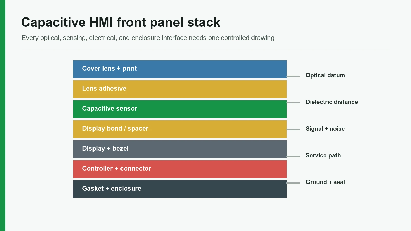
The Industrial HMI Touch Stack, From Operator to Enclosure
An industrial HMI touch stack is the ordered set of optical, dielectric, conductive, adhesive, structural, and electronic layers between the operator and the host system. Not every project needs every layer. A displayless touch keypad may omit the transparent sensor and display; a projected-capacitive display may combine the sensor and controller in a purchased module.
Operator / cleaning medium / glove
Cover lens or rigid front surface Subsurface ink, black mask, icons, surface coating Lens-to-sensor adhesive or controlled gap Capacitive sensor: printed film, FPC, glass/ITO, or PCB electrode Sensor-to-display bond or perimeter spacer LCD / TFT / OLED module and backlight Bezel, carrier, gasket, and compression features Controller PCB, protection, ground/shield connection FPC/FFC/cable, connector, bend and strain relief Enclosure opening, chassis bond, fasteners, and host interface
Equipment reference datum and protective earth/chassis strategy
The touch HMI cover lens is not just decoration. It is a dielectric in the sensing path, an optical surface over the display, a cleaning surface, and often part of the enclosure seal. Its printed border establishes the visible window; its edge geometry meets the bezel; its rear surface receives ink and adhesive. If one lens drawing omits these roles, downstream suppliers will fill the gaps with assumptions.
| Stack element | Drawing must control | Interface to review | Typical failure if omitted |
|---|---|---|---|
| Cover lens and coating | Material, nominal thickness, edge profile, finish, coating zones | Operator, ink, adhesive, bezel | Cracks, glare, cosmetic mismatch, unstable sensing |
| Ink and black mask | Color standard, opacity, registration, cure/process note | Clear window, sensor icons, adhesive | Light leak, blocked display pixels, icon-to-key offset |
| Touch sensor | Technology, active area, electrodes, tail, keep-outs | Lens, display, controller, ground | Weak edge response, false touch, routing conflict |
| Adhesive or spacer | Part number, thickness, geometry, liner, process | Substrates, bubbles, rework, sealing | Newton rings, delamination, trapped contamination |
| Display | Active area, module outline, viewing direction, tolerances | Mask, sensor, carrier, cable | Cropped image, parallax, pressure marks |
| Bezel/carrier/gasket | Datums, flatness, ledges, compression stops | Lens edge, display, enclosure | Bond stress, seal loss, uneven optical gap |
| PCB, ground, connector | Controller, protection, pinout, mounting, bond points | Sensor tail, chassis, host | EMI sensitivity, ESD reset, intermittent cable |
| Enclosure | Opening, fasteners, earth/chassis point, service route | Complete stack | An approved bench sample fails in the machine |
A 10-Point Capacitive HMI Front Panel Design Framework
The ten checks below follow the physical build from enclosure datum to approved assembly. Each check has a acceptance evidence and a release blocker that can be verified on drawings, BOMs, sample records, or test plans.
1. Start With One Enclosure Datum System
Choose the functional origin before artwork begins. A useful scheme might set datum A on the enclosure mounting plane, datum B on a locating edge, and datum C on a hole or molded boss. The lens perimeter, bezel opening, display active area, touch active area, gasket path, connector exit, and fastener pattern then reference A-B-C with tolerances that reflect assembly order.
This prevents “centered” from acquiring three meanings. The display vendor may center the active area within the module, the printer may center the window within the lens, and the mechanical team may center the lens in the enclosure opening. Tolerance accumulation can shift the visible pixels and touch coordinates in opposite directions even though every supplier meets a local drawing.
A stack drawing and coordinate table identify the same functional datums for the enclosure, lens, artwork, sensor, display active area, gasket, and tail exit.
Lens artwork, touch layout, and display drawing use unrelated origins, or dimensions are nominal without positional tolerances.
2. Specify the Touch HMI Cover Lens as an Electrical and Optical Part
Cover material, thickness, permittivity, ink stack, coatings, and local gaps affect sensing; surface finish, refractive interfaces, mask opacity, and viewing angle affect appearance. The drawing should identify glass, polycarbonate (PC), polymethyl methacrylate (PMMA), or another qualified substrate by grade—not only by generic family. It should also separate cosmetic zones from bond and seal zones.
A graphic overlay or printed front needs registration requirements tied to the active sensor and display. Include the clear-window boundary, black-mask overlap, icon center, coating exclusions, edge chamfer/radius, allowable print defects, and inspection lighting. Do not infer chemical resistance from the base substrate; the final printed/coated construction needs its own evidence.
The released lens drawing identifies substrate grade, nominal thickness and tolerance, print side, color/opacity controls, coating zones, window datum, edge finish, and approved cleaning agents.
The RFQ says “tempered glass, black border” while leaving thickness tolerance, ink registration, coating, and cleaner exposure undefined.
3. Match Sensor Architecture to the Interaction
Discrete buttons, sliders, wheels, proximity zones, and a full two-dimensional projected-capacitive matrix solve different problems. Microchip AN2934 separates self-capacitance and mutual-capacitance designs, while Infineon’s 2023 CAPSENSE HMI white paper distinguishes CSD and CSX methods. The correct route depends on channel count, gestures, water behavior, nearby conductors, scan time, controller resources, and sensing distance.
Transparent display sensors often use patterned ITO or another transparent conductor. TI/DAWAR describes ITO deposited on glass or plastic and patterned by photolithography or laser ablation. Displayless keys may use copper on PCB/FPC or printed conductive ink on film. These are architecture choices, not interchangeable BOM substitutions.
A requirement table names each interaction—tap, slider, gesture, proximity—and its operator condition, response criterion, allowable false activation, and host action.
The sensor is chosen only by panel diagonal or visual style, with no decision on wet operation, gloves, neighboring metal, or gesture count.
4. Control Bond Lines, Spacers, and Air Gaps
Every bond line changes geometry. Full optical bonding can reduce internal reflecting interfaces and lock registration, but it also adds lamination process controls, rework consequences, and material compatibility work. Perimeter bonding leaves an air gap that may simplify service or module replacement, yet the gap and spacer flatness must stay controlled. Local voids are neither deliberate optical bonds nor deliberate air gaps.
The named OCA 8211-8215 family includes carrierless acrylic films at 25, 50, 76, 100, and 125 µm. Use 100 µm, corresponding to 3M 8214, as a stack-calculation example only when that product family is under review. The released drawing must name the approved adhesive part, nominal thickness, tolerance, substrate pair, and lamination process.
Each adhesive/spacer has a manufacturer and part number, nominal thickness and tolerance, geometry, liner, surface preparation, storage limit, lamination sequence, and rework rule.
The BOM says “OCA” or “double-sided tape,” and the section drawing does not include its thickness in the tolerance stack.
5. Register the Display, Sensor, Mask, and Bezel Together
The optical datum chain begins at the display’s active pixels, not at the metal frame. The module drawing should distinguish active area, viewing area, polarizer edge, outline, backlight housing, FPC exit, and keep-outs. The front-panel drawing then controls black-mask overlap, sensor border, adhesive edge, bezel ledge, and the enclosure opening relative to those features.
Display viewing direction matters. An LCD intended for one clock orientation can show poor contrast when the installed operator looks from another direction. Thick lenses and air gaps can increase apparent parallax near the display edge. Mechanical pressure from a bezel or gasket can also create display mura or touch baseline shifts, so compression stops belong in the same review.
A common overlay drawing shows display active area, visible window, mask overlap, sensor active area, and bezel opening, with worst-case tolerance analysis.
The display is positioned by its outside metal frame after artwork and sensor tooling have already been approved.
6. Treat the Controller, PCB, Connector, and Tail as Physical Layers
Controller choice cannot wait until the decorative parts are finished. The controller’s sensing topology, channel count, supported shield method, scan behavior, tuning tools, supply, and host interface shape the electrode and routing plan. Renesas documents CTSU/CTSU2 electrode, routing, shielding, wet-operation, and noise work through its capacitive-touch HMI resource hub. Texas Instruments provides equivalent design context through CapTIvate resources.
The mechanical drawing must show FPC or FFC bend zones, stiffener length, insertion direction, ZIF access, minimum service loop, and strain relief. Place connectors so technicians can assemble them without folding the sensor tail against a sharp carrier edge. If a replaceable display and permanent front lens share one cable route, document the service sequence before freezing the carrier.
Controller part/revision, PCB outline, host interface, pinout, connector mating direction, tail bend region, stiffener, strain relief, and programming/tuning access are released together.
The sensor tail ends at an unlabeled rectangle, or the connector is reachable only before the display is bonded into the carrier.
7. Design a Ground, Shield, and ESD Current Path
Ground is not an empty copper area. Ground near electrodes can reduce sensitivity through capacitive loading; too little control can leave traces exposed to display, backlight, switch-mode supply, cable, or chassis coupling. Microchip AN2934 distinguishes passive and active/driven shielding. Renesas’ 2024 noise-immunity guide covers radiated RF, conducted noise, ESD, and electrical fast transients in the context of the IEC 61000-4 series.
A metal bezel needs an electrical definition: floating, capacitively coupled, bonded to chassis, or connected through a controlled network. The design review should trace an ESD event from the touch surface and bezel toward chassis/protective earth without assuming that a TVS diode alone fixes an uncontrolled current path. IEC 61000-4-2:2025 defines ESD immunity requirements and test methods for equipment; it does not certify a loose lens-sensor assembly.
The schematic and mechanical section identify shield/guard regions, chassis bond points, PCB return, transient protection, cable shield termination, and discharge-current paths.
The bezel is marked “metal” with no electrical state, while PCB ground, chassis, and protective earth are treated as interchangeable symbols.
8. Test the Intended Operator and Environment
“Touch works” is incomplete. Record the operator medium—bare dry finger, wet finger, nitrile glove, work glove, approved stylus—and the contamination state. Add temperature, humidity, condensation risk, cleaning residue, nearby motors, inverter cables, display/backlight operating modes, and power-supply conditions expected in the equipment.
A controller can often be tuned for gloves or moisture, but the result is system-specific. Higher sensitivity may narrow the margin to false activation from water, neighboring metal, or coupled noise. The acceptance method should distinguish no touch, valid touch, adjacent-key rejection, held touch, swipe/gesture accuracy, and recovery after contamination or an EMC event.
The test matrix names operator, glove model/material, wetting method, contaminant, temperature state, equipment mode, sample revision, firmware/tuning revision, and pass criterion.
Approval consists of one dry bare-finger demonstration on an open bench with a laboratory power supply.
9. Separate Component Evidence From Finished-Product Validation
A supplier data sheet can qualify an adhesive candidate. It cannot prove the finished HMI’s ingress rating, EMC immunity, chemical resistance, or service life. The 3M OCA 8211–8215 sheet reports internal environmental exposures for that named adhesive family, including +85°C for 500 hours, −40°C for 500 hours, +65°C/95% RH for 500 hours, and 200 thermal-shock cycles from −40°C to +85°C. The same sheet calls its technical data representative or typical rather than specification values.
IEC 60529 classifies enclosure protection. Therefore, an “IP65 lens” is poor language: ingress performance depends on the tested enclosure, gasket path, bond, fasteners, connector exits, pressure equalization, and assembly process. Use quality and testing controls to separate incoming material checks, in-process assembly checks, and end-product validation owned by the OEM.
A responsibility matrix assigns material qualification, front-panel inspection, enclosure ingress testing, EMC testing, software acceptance, and regulatory evidence to named parties and revisions.
A material certificate or supplier brochure is presented as proof that the assembled equipment meets IEC 60529 or IEC 61000-4-2.
10. Freeze a Traceable Approval Package
The golden sample must mean more than “looks good.” Freeze the lens and artwork drawing, stack section, sensor pattern, display/module revision, adhesive BOM, carrier and gasket drawing, PCB and firmware/tuning revision, connector/pinout, cosmetic standard, functional test, packaging method, and approved deviations. Photographs help, but they do not replace measurable criteria.
Change control should identify interfaces affected by each substitution. A new display supplier may preserve diagonal size while moving the active area, polarizer edge, cable, noise spectrum, or frame datum. A replacement OCA may preserve nominal thickness while changing modulus, outgassing response, or substrate adhesion. Requalification depth follows the interface change, not the purchasing label “equivalent.”
The approval record links every sample to controlled drawing, BOM, firmware/tuning, inspection, and validation revisions, with change notification rules.
A sample is signed by appearance only, and production can substitute display, adhesive, or controller parts without interface review.
When a Bonded Capacitive Front Is Not the Best Choice
A bonded capacitive construction is not automatically superior. Choose another route when the equipment requires native mechanical travel, a hard detent that can be confirmed without visual or audio feedback, or actuation with thick work gloves for which no production-stack evidence exists. A membrane switch or silicone keypad may give the operator a clearer physical event.
| Requirement that dominates | Construction to evaluate first | Reason to prefer it |
|---|---|---|
| Flat, sealed display front with gestures | PCAP sensor with bonded or controlled-gap lens | Supports a continuous touch area and display registration |
| Native snap or key travel | Membrane switch or silicone keypad | Provides a physical actuation event without controller-generated feedback |
| Field-replaceable display module | Perimeter-bonded lens with controlled air gap | Separates display service from permanent lens lamination |
| Displayless appliance keys | Printed-film, FPC, or PCB electrodes behind PC/PMMA | Avoids a transparent sensor where no display requires one |
| Safety command requiring independent hardware | Separate mechanical control plus touch HMI | Keeps the critical function outside the touch-only path |
Full optical bonding may also be the wrong process. A perimeter-bonded modular display can be preferable when field replacement, display second-sourcing, low process complexity, or service access outweighs optical benefits. For a displayless appliance panel, printed electrodes behind PC may cost and assemble more sensibly than a transparent ITO sensor. For safety-related commands, the system architecture may require a separate mechanical control regardless of the touch interface.
Use capacitive touch only after defining feedback, failure behavior, contamination, service, and validation. The construction should follow those requirements—not a preference for a flat surface.
From Assembly Drawing to Approved Sample
A controlled release process turns the ten-point framework into documents that suppliers and OEM teams can execute.
Step 1 — Freeze operating inputs before selecting layers
Record display type and active area, operator/glove conditions, gesture or button functions, cleaning agents, indoor/outdoor exposure, target temperature range, expected water state, adjacent noise sources, host interface, service method, and end-product standards. Mark unknowns. An honest “resolved before design verification” is safer than a supplier assumption hidden inside a quotation.
Step 2 — Build one master stack and datum drawing
Create a section through the active display, sensor border, adhesive, lens, bezel ledge, gasket, PCB/carrier, and enclosure. Show nominal dimensions and tolerances. Add top views for artwork, touch coordinates, display active area, and tail exit. A capacitive-touch HMI assembly should be reviewed against this master definition even when several vendors supply its parts.
Step 3 — Release interface control documents
An interface control document should name ownership for display data, touch coordinates, controller-to-host protocol, connector/pinout, ground/chassis points, firmware/tuning revision, and acceptance logs. Include coordinate transform rules if the display, touch controller, and GUI use different origins or rotations.
| Interface record | Minimum controlled fields | Approval output |
|---|---|---|
| Optical coordinates | Display active-area origin, visible window, mask overlap, viewing direction | Registered overlay with worst-case offsets |
| Touch coordinates | Sensor origin, axis direction, rotation, active border, GUI transform | Coordinate map and edge-zone check |
| Electrical connection | Supply, logic levels, protocol, pinout, connector keying | Schematic/ICD revision and continuity test |
| Ground and shield | PCB return, guard/shield net, chassis bond, cable termination | Marked current-path drawing |
| Software baseline | Controller firmware, tuning file, host driver, GUI revision | Version manifest linked to sample serial number |
Step 4 — Build architecture samples before cosmetic tooling
Use representative cover thickness, sensor geometry, display, bezel metal, PCB ground, cable length, and power supply. Appearance details may remain open during architecture sampling, but dielectric distance and noise sources must be representative. Check edge keys, wet states, intended gloves, backlight modes, and nearby switching loads before committing to finished lens printing or high-volume lamination tooling.
Step 5 — Approve cosmetic and dimensional samples
Inspect the printed window, icon registration, mask overlap, coating boundary, lens edge, adhesive line, display alignment, and bezel fit under defined lighting. Measure assembled height and critical XY offsets. Record bubble, particle, scratch, light-leak, and display-pressure criteria with photographs and numeric limits where the project has them.
Step 6 — Run production-intent validation
Use the final enclosure, fasteners, gasket compression, cable routing, controller PCB, power supply, display firmware, GUI, and touch tuning. A useful validation program samples normal operation, corners of tolerance, environmental states, cleaning exposure, mechanical load, ingress targets, and relevant IEC 61000-4 immunity tests. The end-product compliance owner sets levels and acceptance criteria.
Step 7 — Freeze first-article approval and change control
The first-article package links sample serial numbers to drawings, BOMs, process revision, firmware/tuning, inspection data, and validation results. It also lists parts that require notification before change: lens grade, ink, OCA/PSA, sensor conductor, display module, controller, PCB, connector, gasket, and carrier. This record becomes the baseline for incoming inspection and future second-source work.
Validation Matrix and Failure Chains
The matrix below is a planning structure, not a universal test specification. Product safety, regulatory, automotive, medical, marine, and customer standards can add methods or stricter acceptance criteria.
| Validation area | Production-intent conditions | Evidence to retain | Decision owner |
|---|---|---|---|
| Dimensional/fit | Tolerance samples, final bezel, gasket compression, fasteners | CMM/fixture report, stack measurements, photos | Mechanical engineering + supplier quality |
| Optical/cosmetic | Defined lighting, viewing angles, display states, clean and aged samples | Window registration, luminance/contrast if specified, defect record | Industrial design + display engineering |
| Touch function | Approved gloves, wet/contaminated states, edge zones, gestures, full cable/power configuration | Raw counts/baselines where available, event logs, tuning revision | Electronics/firmware engineering |
| Mechanical/environmental | Temperature/humidity corners, cleaning agents, vibration/drop/load as applicable | Sample revision, method, dwell/cycles, before/after results | Reliability engineering |
| Ingress | Complete enclosure, production gasket/bond, connector exits, specified mounting | IEC 60529 test report for the tested configuration | End-product compliance owner |
| EMC/ESD | Final enclosure, chassis bonds, display/backlight modes, cables, power states | IEC 61000-4 setup, level, criterion, event log | EMC/compliance engineering |
| Production process | Approved materials, lamination, cure, cleanliness, fixtures, operator instructions | Traveler, lot trace, in-process and final inspection | Manufacturer + supplier quality |
| Observed symptom | Likely stack/interface causes | Confirmation method |
|---|---|---|
| Edge key misses | Mask/sensor offset, bezel loading, local gap, ground proximity | Overlay coordinate measurement; raw channel scan with bezel installed |
| False touch when wet | Water bridge, tuning margin, shield pattern, seal residue | Controlled wetting map; compare dry/wet baselines and adjacent channels |
| Reset during ESD | Uncontrolled bezel path, cable coupling, poor chassis bond, protection layout | Current-path review; IEC 61000-4-2 pre-compliance on final enclosure |
| Bubbles after heat/humidity | Substrate outgassing, contamination, OCA mismatch, lamination void | Cross-section/visual map; material and process lot review; conditioned samples |
| Display window appears shifted | Independent datums, module active-area tolerance, mask registration | Worst-case datum stack; measure active pixels to lens references |
| Touch changes with backlight load | Display/backlight noise, supply ripple, routing, scan frequency | Compare raw data across display brightness and power modes |
| Seal passes flat-panel check but leaks in product | Gasket compression, fastener pattern, enclosure warp, cable exit | Full-enclosure ingress test; compression-film or witness-mark review |
Drawing and Sample-Approval Checklist
Send the display and front-panel assembly drawing early. The first review should include the items below; missing files can be identified as open with an owner and due date.
- [ ] Enclosure STEP/DXF/PDF with A-B-C datums, opening, fasteners, chassis/earth points, and allowed assembly sequence.
- [ ] Display manufacturer and module drawing with outline, active area, viewing area/direction, polarizer, FPC, and keep-outs.
- [ ] Lens drawing with substrate grade, nominal thickness/tolerance, edges, coatings, print side, artwork, black mask, and cosmetic zones.
- [ ] Touch requirement map: buttons/sliders/gestures, coordinates, glove/wet conditions, feedback, and false-activation limits.
- [ ] Sensor construction, active area, tail, electrode keep-outs, shield/guard concept, and controller family.
- [ ] Adhesive/spacer BOM with part numbers, nominal thickness/tolerance, geometry, preparation, liner, and lamination route.
- [ ] Bezel/carrier/gasket drawing with flatness, compression stops, display support, lens support, and service access.
- [ ] PCB schematic/layout, connector/pinout, FPC bend/stiffener, cable length, chassis bond, and protection devices.
- [ ] Host interface and firmware/tuning revision, coordinate transform, diagnostic data, and update method.
- [ ] Validation plan assigning component checks, assembly checks, IEC 60529, IEC 61000-4, chemical, mechanical, and application-specific work.
- [ ] Golden-sample record and change-notification list.
- [ ] Approved adhesive part, thickness, tolerance, substrate pair, and lamination process replace the 100 µm calculation example in the released drawing.
For an integration review, the project team can send the display and front-panel assembly drawing. Include the enclosure section and cable/ground plan, not just lens artwork. A related capacitive touch control-panel application can help teams identify which interface details to document, even if that planned route is not yet live.
Frequently Asked Questions
What layers belong in a capacitive HMI front panel stack-up?
A typical stack includes the cover lens, rear graphics or black mask, lens adhesive, capacitive sensor, sensor-to-display bond or spacer, display, bezel/carrier, gasket, controller PCB, connector tail, and enclosure. Displayless key panels omit the display layers. The released drawing should identify every actual interface and its datum.
Should the touch sensor be bonded to the cover lens or left with an air gap?
Neither route is universally correct. Bonding can lock registration and reduce internal optical interfaces; a controlled air gap can simplify display service and rework. Compare optical needs, sensing margin, process capability, contamination control, field replacement, and reliability evidence using production-intent samples before choosing.
How thick should the touch HMI cover lens be?
There is no universal thickness. Lens material, dielectric properties, sensor geometry, controller, glove requirement, edge support, impact load, coating, and optical target interact. Select a preliminary range from supplier capability, then prove touch margin and mechanical performance on the actual stack. Do not copy a smartphone or competitor dimension without validation.
Can one capacitive front panel assembly work with gloves and water?
It can, provided the sensor, controller, shield, grounding, firmware, and enclosure are designed and tested for the named glove and water condition. “Glove” should identify material and thickness; “wet” should define the liquid and method. Approval with a dry bare finger does not demonstrate either requirement.
Where should the touch controller sit?
Place the controller within the selected sensor vendor’s routing, parasitic-capacitance, noise, service, and thermal constraints. Short, controlled sensor traces are generally easier to manage than long unshielded runs, but the final location must also support connector access, chassis strategy, firmware updates, display routing, and assembly sequence.
How should the display, sensor, and artwork be aligned?
Reference them to one functional datum system. The overlay should show display active pixels, visible window, black-mask overlap, sensor active area, touch coordinates, bezel opening, and worst-case tolerances. Do not align the display only by its outside frame; module and active-area offsets can differ.
Does an IP-rated front panel make the finished HMI IP rated?
No. IEC 60529 classifies enclosure protection in the tested configuration. Lens bonds, gasket compression, fasteners, enclosure flatness, connector exits, vents, and assembly process affect the result. A front component may support an ingress target, but the finished enclosure must be tested and documented by the responsible product owner.
Which standards are relevant to an industrial HMI touch stack?
Common references include IEC 60529 for enclosure ingress classification and the IEC 61000-4 series for EMC immunity methods, including IEC 61000-4-2 for ESD. Product, market, safety, medical, automotive, and marine requirements can add standards. The compliance plan must set editions, levels, configurations, and acceptance criteria.
What files should an OEM send before design review?
Send the enclosure and front-panel assembly drawing, display module drawing, lens artwork, touch map, operator/environment requirements, adhesive concept, bezel/gasket section, controller and PCB information, connector/pinout, chassis/ground plan, and target validation standards. Mark unfinished inputs with an owner and decision date rather than leaving silent assumptions.
Technical References
- Source: Microchip AN2934 Capacitive Touch Sensor Design Guide. Accessed 2026.
- Source: Infineon AN85951 CAPSENSE Design Guide. Accessed 2026.
- Source: 3M OCA 8211-8215 Technical Data. Accessed 2026.
- Source: Renesas Capacitive Touch HMI Design Guidance. Accessed 2026.
- Source: IEC 60529 Degrees of Protection Provided by Enclosures. Accessed 2026.
- Source: IEC 61000-4-2:2025 Electrostatic Discharge Immunity. Accessed 2026.
- Source: AN2934 Capacitive Touch Sensor Design Guide. Accessed 2026.
- Source: transparent capacitive-touch paper. Accessed 2026.
- Source: integration scope. Accessed 2026.
- Source: CAPSENSE HMI white paper. Accessed 2026.
- Source: OCA 8211–8215 data sheet. Accessed 2026.
- Source: capacitive-touch HMI resource hub. Accessed 2026.
- Source: IEC 61000-4-2:2025. Accessed 2026.
- Source: IEC 60529. Accessed 2026.
Review the complete capacitive touch stack before release
Send the cover, artwork, active area, display, electrode, controller, tail, environment, and acceptance states for an engineering review.