
Good backlit silicone keypad design treats the legend, coating, silicone, light-control features, LED, PCB, and housing as one optical stack. Select the construction from the required lit and unlit appearance, then approve it on a complete powered sample; no universal LED spacing, pigment dose, or laser depth can replace that test.
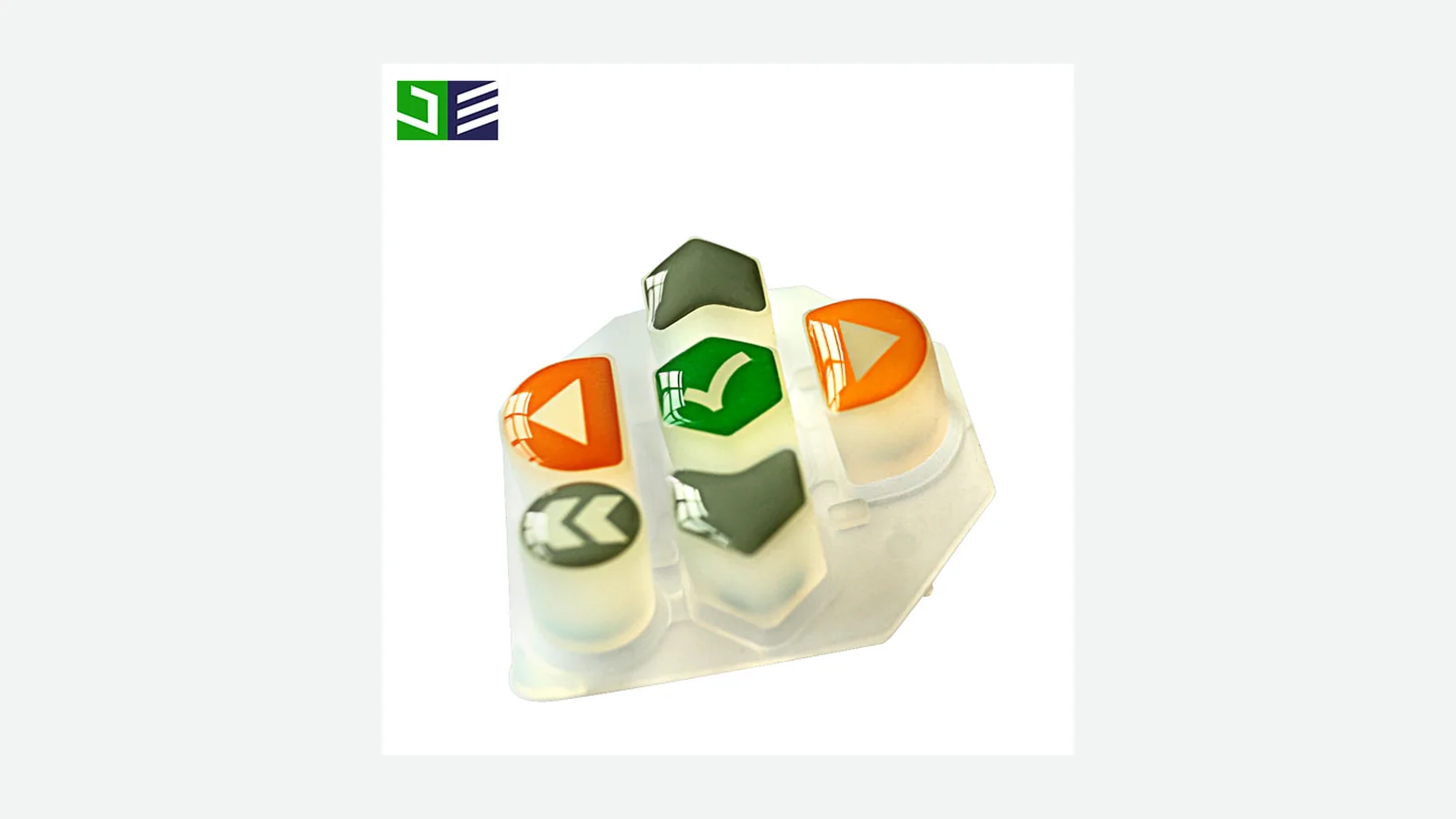
This guide decides when to use a laser-opened coating, a molded silicone light pipe or window, direct LED illumination, or a separate light guide. It is written for OEM engineers and technical buyers who must coordinate artwork, rubber geometry, PCB layout, drive electronics, and enclosure details before tooling. The boundary is equally important: supplier datasheets establish input conditions, while the assembled keypad establishes the visible result. Teams comparing backlit silicone rubber keypads should use the nine checks and six-step approval process below before releasing the PCB or cosmetic tooling.
1. Why This Decision Matters
A weak backlight decision becomes expensive because its causes sit in different owned parts. The legend belongs to artwork. The coating and silicone belong to the keypad. The source and current belong to the PCB. Masking may belong to a spacer or enclosure. Once tooling, routing, and cosmetic approval split across those teams, a bright dot can require more than an LED change.
A common laser-etched stack looks like this:
operator and ambient light
clear protective coat, if required
opaque cosmetic / light-blocking coating
laser-opened legend aperture
translucent or diffusing silicone key body
optional molded light block, window, spacer, or guide
LED package + resistor / driver on PCB
housing cavity and partitions
The sequence is documented by both JASPER's laser-etched keypad description and CSI Keyboards' coated-rubber process. It is common, not mandatory. A full-glow key, isolated status window, dead-front icon, or wide illuminated field may need a different exit path.
The visible symptom is rarely the root cause
| Visible symptom | Likely stack causes | Verification that separates them | Release action |
|---|---|---|---|
| Bright dot inside a legend | Short optical path, narrow or nonuniform LED pattern, clear key body, insufficient mixing | Luminance map with the final LED; compare one material or standoff change at a time | Revise source position, diffusion, cavity, or guide—not merely current |
| Dim corners or a long legend fading at one end | Source footprint too small, obstruction by stem or contact, inadequate guide extraction | Angular LED data plus an assembled sample with point measurements | Offset, reorient, distribute, or couple the source after checking the mechanical stack |
| Adjacent key glows when only one channel is on | Shared translucent base, coating pinhole, missing opaque rib or housing partition | Energize one channel at a time and measure the neighboring OFF region | Add a controlled light barrier and repeat the single-channel test |
| Nominally white keys have different tints | Mixed LED color bins, current or temperature shift, silicone/coating spectral effect | Record LED bins; measure assembled chromaticity at the specified current and temperature | Restrict or qualify bin combinations and lock the optical stack |
| Jagged, dim, or inconsistent legend edge | Residual coating, excessive ablation, artwork feature too fine, topcoat interaction | Inspect unpowered edges, powered emission, and a process-ladder coupon | Qualify a coating-removal window and accepted residual/substrate condition |
| Halo around bezel or key perimeter | Coating gap, aperture clearance acting as a light slot, reflective housing wall | Inspect with the production bezel and controlled exposure, not a loose keypad | Extend masking, darken the aperture wall, or alter the overlap geometry |
LED datasheet brightness does not close these questions. Nichia distinguishes directional luminous intensity, total luminous flux, and apparent-surface luminance; the finished legend is an emitting surface, not the bare LED package. Simple inverse-square reasoning can fail at short distances with nonuniform source directivity. See Nichia's brightness and color application note.
The practical thesis is simple: freeze the visible requirement first, preserve the full optical path in one controlled data set, and make the powered assembly—not a CAD render, loose rubber mat, or typical LED curve—the approval authority.
2. The Nine-Point Backlit Silicone Keypad Design Framework
The framework runs in dependency order: viewing conditions, silicone and color, light-exit architecture, laser process, LED placement, mechanical obstructions, light containment, electrical/thermal control, and sample approval. A later check cannot rescue a missing earlier input without a board, tooling, coating, or artwork change.
2.1 Define the lit and unlit viewing conditions
Start with the appearance states, not an LED part number. For every key or indicator, identify what must be visible with power OFF, what must appear with power ON, and whether the illumination communicates a functional state. Record ambient illumination, viewing distance and angle, production drive current, supply tolerance, enclosure finish, temperature condition, and the region on which measurements will be taken.
“Uniform” also needs a declared calculation. CIE S 017:2020 defines luminance uniformity, Uo, as minimum luminance divided by average luminance over a surface. If a project instead uses minimum/maximum, coefficient of variation, or a key-to-key ratio, name that metric rather than labeling it CIE Uo. The target value remains an OEM decision because a status dot, a long text legend, and a full-glow key do not have the same visual task.
The drawing or appearance specification defines OFF, ON, and single-channel states, measurement regions, geometry, ambient condition, electrical condition, and numerical acceptance fields.
The only requirement is “even white backlight,” a rendering, or a maximum LED mcd value.
2.2 Specify silicone optical behavior and color as a system
“Transparent silicone” is not a usable optical specification. WACKER's silicone processing guide describes formulations ranging from transparent through translucent to opaque. Grade, optical path length, surface finish, pigment or diffusant, cure, and wavelength or luminous-transmittance method all change what a number means.
Supplier data show the boundary clearly. Dow lists 92% luminous transmittance at 10 mm for SILASTIC MS-1003, an optical molding grade offered for light pipes and guides. That value establishes feasibility for that named grade and condition; it does not predict a coated keypad or prove suitable tactile and tear properties. WACKER's ELASTOSIL color-paste TDS gives a 0.5–4.0% range for one named paste ; excess can slow cure. It is evidence that pigment dose is product specific, not a recipe to copy.
Haze and transmission are separate. ASTM D1003-21 distinguishes haze from luminous transmittance for suitable planar, essentially transparent specimens. Haze redistributes light; it is not an efficiency score. A textured, colored, curved keypad still needs an assembled optical test.
The material callout ties a named compound and color system to plaque thickness, finish, cure, transmittance/haze method where applicable, and final-key approval.
A Pantone reference, the word “milky,” or a supplier's best-case transmission percentage is treated as the complete powered-color specification.
2.3 Choose the light-exit architecture before tooling
The right construction depends on where light must travel and where it must stop. A laser etched backlit keypad is one option, not the default answer to every illuminated HMI.
| Construction | Use it when | Principal control | When it is not the best choice |
|---|---|---|---|
| Translucent key body + opaque coating + laser-opened legend | Selective text or icons need a dark surrounding key face | Coating opacity, ablation window, local diffusion, and legend-to-source alignment | Full-area glow, large uniform fields, or unlit multicolor graphics dominate the requirement |
| Opaque base + insert-molded translucent window or silicone light pipe | An indicator or key needs stronger optical isolation from adjacent features | Insert geometry, coupling, boundary contact, and molder-specific tolerances | Tooling simplicity, very fine graphics, or easy late artwork changes matter more than isolation |
| Direct LED into a diffusing translucent key or window | A compact key or indicator can mix light within its available cavity | LED angular pattern, standoff, obstruction, material scatter, and masking | A wide legend, very short path, or an opaque central contact leaves no mixing volume |
| Separate edge-lit guide or light-guide film | Light must spread across a larger field from side-coupled sources | Coupling face, mixing range, extraction pattern, films, openings, and housing pressure | Independent per-key states, thick interruptions, or a small isolated indicator make the guide unnecessarily complex |
ams OSRAM AN072 explains that radiation pattern, pitch, guide geometry, material, extraction structures, and diffuser films jointly control a guide's mixing and uniformity. Dow explicitly lists light-pipe and light-guide uses for MS-1003. For molded windows, a 0.060 in minimum light-pipe size and several 0.030 in window/edge rules—but those are SiTECH process limits, not universal values or verified JASPER limits.
Laser etching is also a poor fit when the icon should be invisible while unpowered but must remain independently legible for a safety function. A dead-front effect deliberately removes unlit visibility; that trade belongs in the HMI risk decision, not in a cosmetic review.
A construction decision table is approved before the mold, PCB, and legend artwork are released.
“Use laser etching” is chosen because it appears durable, with no powered/unpowered view, stack, or alternative documented.
2.4 Control laser etching by outcome, not a universal depth
Laser opening is selective coating removal. TRUMPF's laser-decoating description explains the absorption-driven removal mechanism, while layer-by-layer selectivity depends on coating composition and laser parameters. Neither source supplies a transferable keypad depth—and that is the point.
The production specification should define the accepted result: no residual light-blocking film in the legend, no exposed pinholes outside it, controlled edge shape, no visible substrate charring or gouging, compatible protective topcoat, and repeatable lit output. A laser ladder or coupon on the actual silicone/coating/topcoat stack can bracket the usable process window before final legend cosmetics are frozen. Cross-section or magnified inspection may help explain a failure, but powered appearance remains part of acceptance.
The first-article record links coating batches, laser program revision, coupon settings, unpowered microscopy, and powered inspection.
A micrometre depth, power percentage, or pass count copied from another color stack is treated as a material-independent drawing value.
2.5 Place LEDs from angular data and the physical stack
An LED rubber keypad drawing that shows only an X–Y center coordinate is incomplete. The optical input includes package height and orientation, angular-intensity curves, rayfile origin, intensity and color bins, drive current, temperature, solder tolerance, and the location of stems, contacts, spacers, and housing walls.
| LED input | Why it changes the keypad result | Release evidence |
|---|---|---|
| Top-emitting or side-emitting package and mounted height | Changes the entry face, footprint, shadowing, and coupling path | PCB land pattern, 3D envelope, polarity/orientation, assembly tolerance |
| Full horizontal and vertical angular-intensity data | A headline viewing angle is only one point on the curve, not a uniform cone | Supplier datasheet or qualified rayfile tied to the exact orderable part |
| Intensity and color-bin range | The same family can ship across allowed ranges rather than one exact output | BOM bin field, approved combinations, reel/lot traceability plan |
| Current, duty cycle, junction or solder-point temperature | Output and chromaticity can move away from datasheet test conditions | Driver schematic, worst-case electrical analysis, temperature validation point |
| Final silicone, coating, spacer, bezel, and housing | External optics absorb, scatter, extract, or block the package output | Complete-stack simulation or representative bench mule, then first article |
The viewing-angle caveat is concrete: an ams OSRAM KRBT QDLP61.3A datasheet lists 120° as a typical half-intensity angle for that device. It does not promise a uniformly illuminated 120° cone. Nichia's near-field guidance is why center placement or inverse-square estimates cannot be promoted to a universal rule.
PCB and keypad teams review the same 3D stack, selected LED data, obstruction map, and powered prototype before routing lock.
The LED is centered under the key after routing because “wider angle means more uniform.”
2.6 Resolve the switch mechanics and light path together
The light source competes with the switching mechanism for volume. A carbon contact, pusher stem, tactile switch, metal dome, support wall, adhesive spacer, vent channel, or guide opening can sit directly in the desired path. Moving an LED can cure one shadow and create another; thinning a key top can alter molding or feel; cutting an air channel through a guide can produce a bright extraction edge.
Map these items on a shared section through every distinct key family, not only a plan view. Wide rocker keys, long legends, and keys with asymmetric contacts deserve separate sections. The Niceone-HMI design guide documents the practical conflict between opaque contacts and the optical path; the claim is used as manufacturer process evidence, not as a source for universal spacing.
Each key family has a section showing legend aperture, key-wall thickness, contact or dome, LED package envelope, vent path, guide/spacer, PCB, bezel, and tolerances.
The artwork, rubber drawing, and PCB are individually correct but have no controlled common datum or section.
2.7 Contain light through coating, molding, spacer, and housing
Light leakage is a stack problem. An opaque coating controls surface emission; an opaque molded base or insert can isolate a window; a dark spacer limits lateral travel near the PCB; a housing partition can shadow the bezel gap. Selecting one control without inspecting the others invites cross-glow or a perimeter halo.
SiTECH's insert-molding description identifies optical isolation as a reason to mold translucent inserts inside opaque silicone. The alternative can be a coated translucent mat with local barriers, but coating pinholes and flex zones then become optical inspection features. For state-signaling keys, test one LED channel at a time; an “all keys ON” photograph hides cross-glow.
Do not turn sealing potential into an IP claim. IEC 60529 classifies protection provided by enclosures. A loose keypad cannot establish the installed interface's rating; the defined keypad–bezel–gasket–housing assembly is the test boundary.
The optical control plan assigns each leak path to a named coating, molded feature, spacer, or enclosure surface and verifies isolated channels.
Light bleed is judged on a loose keypad, while the IP claim is assigned to that same loose part.
2.8 Control LED bins, drive, temperature, and assembled color
Part-family identity does not guarantee one brightness or color. The ams OSRAM KRBT QDLP61.3A example is sold across documented intensity groups; Nichia datasheets also bind ranks to stated current, pulse, and temperature conditions. A production BOM should state the exact orderable part, permitted intensity and color bins, or the qualified combinations that the finished keypad can tolerate.
Dimming method matters. LED intensity does not necessarily scale linearly with forward current, and amplitude changes can shift chromaticity. PWM at a fixed on-state current can reduce that particular source of color movement, but it does not erase peak-current, thermal, flicker, camera, EMC, or driver constraints.
For RGB or color-critical work, ams OSRAM AN117 calls for measurement of each die's intensity and CIE color point and temperature adjustment. Cree LED likewise documents that current, temperature, and external optics affect final color. Their product-specific numbers are not keypad limits; the shared lesson is to measure the assembled optical stack at operating conditions.
BOM bins, drive mode, current tolerances, thermal condition, and assembled chromaticity checks are under revision control.
Samples use hand-selected LEDs or a laboratory supply that does not match production drive electronics.
2.9 Make the assembled optical sample the approval authority
Approve numbers and appearance together. A useful first-article record includes raw point data, a labeled measurement map, instrument and geometry, stabilization time, ambient condition, drive settings, temperature, LED lot/bin, keypad and coating lot, laser program, housing revision, and high-resolution reference images with fixed exposure. Images locate defects; they do not replace a luminance or color record.
Color method also needs care. CIE 015:2018 and ISO/CIE 11664-3:2019 provide the colorimetric framework for self-luminous, transmitting, and reflecting stimuli. ISO/CIE 11664-6:2022 excludes areas perceived as primary light sources from CIEDE2000's scope. Therefore, the project must classify the lit legend and agree on chromaticity or color-difference coordinates before setting a tolerance. Off-state object color may use a different method, with specimen texture and gloss controlled as ASTM D2244-25 requires buyer and seller to agree.
The approved sample links numerical data, production-representative parts, and an explicit change-control rule.
Approval is an emailed phone photo labeled “looks good,” with no record of LED bin, current, exposure, housing, or ambient light.
3. Step-by-Step Buyer Process
This sequence turns the framework into controlled inputs and evidence. It starts before the RFQ, keeps the keypad, PCB, and housing on one revision path, and ends with a numerical golden-sample record. Skipping the middle steps merely moves discovery into expensive tooling or production builds.
Step 1 — Freeze use conditions and appearance states
Write an optical requirements page for each key family or indicator class. It should answer four groups of questions:
| Requirement group | Inputs to freeze before architecture selection |
|---|---|
| User and environment | Viewing distance and angle; ambient-light range; dark adaptation if relevant; gloves; expected OFF-state legibility |
| Lit behavior | Always on, dimmable, state-signaling, flashing, RGB/multicolor, dead-front, or separate indicator; which adjacent channels may be OFF |
| Electrical and thermal | Supply range, driver or resistor topology, current/duty limits, startup state, intended operating temperature condition |
| Acceptance | Luminance regions, uniformity formula, color coordinates/method, light-bleed and cross-glow regions, cosmetic limits, sample quantity |
Do not borrow a display, automotive, medical, or military limit unless the finished-product requirement actually invokes it. The keypad component team needs the applicable limit and test condition, not an unsupported industry label.
Step 2 — Release one coupled keypad–PCB–housing data pack
Issue the RFQ with vector legends and source files, not screenshots. Add the rubber 2D/3D model, PCB Gerber or CAD, LED BOM candidate, schematics or drive settings, bezel and housing sections, coating/color intent, and the operating-environment requirement. Give every file a revision.
The drawing checklist below catches the gaps that cause most optical rework:
| Controlled item | Minimum data in the release | Primary owner |
|---|---|---|
| Legend artwork | Vector path, size, stroke/negative space, location datum, lit color, OFF-state appearance | Industrial design / HMI |
| Silicone keypad | Key sections, optical regions, compound/color callout, wall and mat geometry, contacts, vents, inserts, coating zones | Mechanical + keypad supplier |
| PCB and LEDs | Exact orderable LED, package/orientation/height, bins, current, driver, resistor tolerance, placement tolerances | Electrical engineering |
| Light control | Opaque ribs, masks, spacer color, guide/extraction features, bezel overlap, housing-wall finish | Mechanical / optical |
| Approval plan | Measurement map, instrument/geometry, ambient, electrical/thermal state, numerical fields, cosmetic views | Quality + system engineering |
If the supplier will deliver the rubber, circuit, LEDs, and connector as one module, the silicone keypad assembly route may reduce interface ambiguity. It does not remove the need for controlled OEM requirements.
Step 3 — Simulate the chosen source, then build a representative mule
Use optical simulation when the geometry, guide, or source count justifies it. Import the correct rayfile orientation and flux assumptions; example spectra and rayfiles do not guarantee the exact spectrum of every delivered LED or bin. Simulation should rank design directions, not create false production precision.
Follow it with a bench mule that uses the candidate package, production-like drive electronics, intended optical path length, representative silicone or plaque, mask, and enclosure surfaces. Vary one factor at a time: source offset, standoff, diffusion, extraction pattern, or barrier. For wide-area alternatives, compare the direct-LED route with the site's backlighting options guide before locking per-key sources.
Step 4 — Approve plaques and a coating/laser process ladder
Material plaques should reproduce the proposed compound, pigment or diffusant, cure/post-cure, thicknesses, and surface finishes. Record both reflection/off-state color and transmitted/on-state color because one visual chip cannot specify both. For applicable planar specimens, record transmittance and haze together under a named method; never read haze as optical efficiency.
The coating/laser ladder should bracket acceptable removal across actual layers. Inspect residual coating, legend edge, pinholes, substrate condition, topcoat appearance, and powered emission. Retain the settings and images linked to material batches. A supplier that performs molding, coating, and laser work under one controlled review can shorten feedback; JASPER's manufacturing capabilities are one option to assess, not evidence of an SK-010 result.
Step 5 — Inspect complete first articles with a defined optical matrix
Run first articles with the production PCB revision, allowed LED bins, production drive, keypad, spacer, bezel, and housing. Use the site's testing and validation planning page to coordinate component and assembly evidence. The matrix below contains fields, not universal limits; the OEM must enter its own target and sampling plan.
| Test / view | Controlled condition | Record | Project acceptance field |
|---|---|---|---|
| OFF-state appearance | Defined illuminant/ambient, angle, distance, clean dry surface | Color coordinates or agreed object-color result; legend contrast; gloss/texture notes | OEM value / visual master |
| ON-state legend luminance | Production current and warmed/stabilized assembly; defined measurement grid | Raw point luminance, average, minimum, maximum, map | OEM range |
| Within-legend uniformity | Same grid and region of interest | CIE Uo or other explicitly named formula | OEM ratio |
| Key-to-key balance | Same-function keys, same drive state | Per-key average and ratio/difference | OEM limit |
| Lit color | Declared CIE/ISO coordinate method, instrument, geometry, temperature | Chromaticity coordinates and LED/bin/lot | OEM window |
| Light bleed and bezel halo | Normal channel ON; neighboring regions defined | Maximum or mapped stray luminance plus fixed-exposure image | OEM limit |
| Cross-glow | One state-signaling channel ON at a time | ON key and adjacent OFF-key values; contrast calculation | OEM ratio |
| Viewing envelope | Specified angles/distances and ambient states | Pass/fail with values where required | OEM envelope |
For an internal example of controlling both light states and LED indicators, see JASPER's backlit panel with LED indicators case page. Treat it as related navigation, not independent proof for this keypad.
Step 6 — Lock the golden sample, data record, and revalidation triggers
A golden sample without its conditions is decoration. Link the physical sample ID to raw optical data, photographs, instrument settings, PCB and housing revisions, LED order code and bins, material/coating lots, laser program, and deviation record. Define who owns it, how it is stored, and when it expires or is replaced.
Change control should trigger review for LED die/package/bin changes, resistor or firmware changes, compound/pigment/coating/topcoat changes, laser-program updates, mold repair, wall-thickness or finish changes, spacer/adhesive changes, PCB stack/placement changes, and enclosure color or geometry changes. Environmental validation must name the exact method and severity. IEC 60068-2-14:2023 covers change-of-temperature methods; IEC 60068-2-78:2025 covers steady damp heat. Neither supplies a universal keypad cycle or pass criterion.
4. Release Blockers That Disqualify a Supplier
These failures override an attractive sample photograph or a low quotation. Each one breaks traceability between the released design and the visible result.
- Promises a universal LED spacing or one LED per key without the selected package and stack — source geometry, obstruction, diffusion, and legend shape determine the footprint.
- Quotes a generic “transparent silicone” with no grade, color system, thickness, cure, or optical-coupon plan — the material cannot be reproduced or compared.
- Treats Pantone, RAL, or a phone image as the powered-color specification — reflected object color and emitted legend color are different approval states.
- Sets laser depth from an old project without a coating/laser ladder — selective ablation depends on the actual coating, silicone, topcoat, and process parameters.
- Samples with hand-picked LEDs or an adjustable bench supply but omits production bins and drive — the approved appearance is disconnected from the BOM.
- Shows all LEDs ON during light-bleed review — cross-glow between independently controlled channels becomes invisible.
- Approves loose rubber while ignoring the bezel, spacer, PCB, and housing — the tested optical boundary is incomplete.
- Claims an IP code for the loose keypad or says “IEC 60068 compliant” without a specific part, severity, specimen state, and report — the supplier is confusing a material or method with an assembled-product result.
- Will not provide raw point data, settings, lot/revision identifiers, and change triggers with the golden sample — future production cannot be compared to the approval evidence.
5. Frequently Asked Questions
What is the best method for backlit silicone keypad design?
The best method is the construction that meets both powered and unpowered appearance requirements on the final assembly. Laser-opened coatings suit selective legends; molded windows or light pipes improve isolation; direct LEDs suit compact optical paths; and a separate guide suits a wider field. Decide before tooling, then approve the actual PCB, keypad, spacer, bezel, and housing together.
When should you use a laser etched backlit keypad?
Use a laser etched backlit keypad when selected icons or text must transmit through an otherwise opaque key face. The method is especially useful when the legend artwork can be opened in a qualified coating stack. It is not automatically best for full-key glow, broad uniform fields, unpowered multicolor graphics, or any design that cannot tolerate a coating process.
Is a silicone light pipe better than placing an LED directly under a key?
A silicone light pipe is better when light must be routed, isolated, or delivered to a window that is not directly above the source. A direct LED can be simpler for a compact key with enough mixing distance and no central obstruction. Neither is universally brighter or more uniform; coupling, boundaries, geometry, material, source pattern, and the assembled housing decide the result.
How many LEDs does a rubber keypad need, and where should they go?
There is no universal LED count or placement rule. Start with the selected LED's horizontal and vertical angular-intensity data, package orientation and height, legend geometry, optical path, diffusion, contacts or domes, and allowed current. Model or bench the candidate layout, then verify luminance and cross-glow on production-representative first articles.
How is backlight uniformity measured on a keypad legend?
Define the legend's region of interest and measurement points, stabilize the complete powered assembly, then record luminance at each point under controlled geometry and ambient conditions. CIE S 017:2020 defines luminance uniformity Uo as minimum divided by average luminance. If the project uses minimum/maximum or another equation, name it and set a project-specific limit.
Can a Pantone or RAL color specify the illuminated legend color?
No. Pantone or RAL can communicate an off-state surface-color intent, but the illuminated color also depends on LED spectrum and bin, drive current, temperature, silicone grade, pigment, thickness, coating, and the optical path. Approve off-state object color and on-state chromaticity as separate conditions using agreed instruments, geometry, and tolerances.
What laser depth should be specified for a backlit silicone legend?
Do not specify a universal depth. Define the accepted result: complete removal of the blocking layer within the legend, no pinholes outside it, controlled edges, no unacceptable substrate damage, compatible topcoat, and repeatable powered output. Qualify a process window with a laser ladder or coupon made from the actual silicone and coating stack.
What files should be sent before tooling a backlit silicone keypad?
Send vector icon artwork, target lit and unlit colors, the keypad 2D/3D model, key sections, PCB layout, exact LED candidates and bins, drive schematic or current settings, spacer and housing sections, operating conditions, and an optical acceptance matrix. The icons, colors, and PCB LED layout should be reviewed as one release package.
6. What to Do Next
Freeze the two appearance states, choose the light-exit architecture, release the keypad–PCB–housing stack, and define the optical matrix before cosmetic tooling. The next practical package is compact: share the vector icons, target colors with LEDs OFF and ON, keypad sections, exact LED candidates, drive method, and PCB LED layout. Add the housing and spacer sections if light containment matters—which it usually does.
Send the coupled artwork, keypad, PCB, LED, drive, spacer, housing, and optical acceptance package through the project contact route. The review must close both the powered and unpowered appearance before cosmetic tooling is released.
Technical References
- Source: Nichia Key Characteristics of Light Brightness and Color. Accessed 2026.
- Source: Nichia LED Luminous Intensity Control Note. Accessed 2026.
- Source: ams OSRAM LED Rayfile Application Note AN086. Accessed 2026.
- Source: TRUMPF Laser Decoating Guidance. Accessed 2026.
- Source: WACKER ELASTOSIL Color Paste Technical Data. Accessed 2026.
- Source: Dow SILASTIC MS-1003 Optical Silicone Data. Accessed 2026.
- Source: CSI Keyboards' coated-rubber process. Accessed 2026.
- Source: brightness and color application note. Accessed 2026.
- Source: CIE S 017:2020. Accessed 2026.
- Source: WACKER's silicone processing guide. Accessed 2026.
- Source: SILASTIC MS-1003. Accessed 2026.
- Source: ELASTOSIL color-paste TDS. Accessed 2026.
- Source: ASTM D1003-21. Accessed 2026.
- Source: ams OSRAM AN072. Accessed 2026.
- Source: SiTECH's Application Guide. Accessed 2026.
- Source: TRUMPF's laser-decoating description. Accessed 2026.
- Source: Fraunhofer IFAM. Accessed 2026.
- Source: KRBT QDLP61.3A datasheet. Accessed 2026.
- Source: Nichia's near-field guidance. Accessed 2026.
- Source: Niceone-HMI design guide. Accessed 2026.
- Source: SiTECH's insert-molding description. Accessed 2026.
- Source: IEC 60529. Accessed 2026.
- Source: Nichia's 2026 intensity-control note. Accessed 2026.
- Source: ams OSRAM AN117. Accessed 2026.
- Source: current, temperature, and external optics affect final color. Accessed 2026.
- Source: CIE 015:2018. Accessed 2026.
- Source: ISO/CIE 11664-3:2019. Accessed 2026.
- Source: ISO/CIE 11664-6:2022. Accessed 2026.
Review the complete keypad stack before release
Send the keypad drawing, contact geometry, PCB artwork, environment, appearance targets, and validation plan for a project-specific review.