
Rubber keypad PCB contact design succeeds when pad geometry, pill size, worst-case alignment, surface finish, delivered force, contamination, and the sensing circuit are specified as one system. This guide helps PCB, HMI, mechanical, validation, and sourcing teams release a low-energy carbon-pill interface. Both nets must remain inside the pill's guaranteed overlap zone, and the production-intent assembly must pass a defined electrical test at controlled force and travel. The method does not rate a carbon pill as a power switch, set a universal life value, or replace validation of the finished equipment.
1. Define the Contact Stack Before Drawing Copper
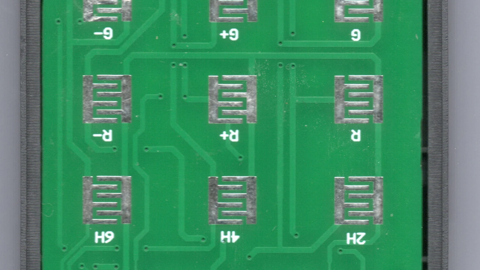
A conductive rubber key is a normally open momentary switch. The silicone web supplies motion and return force; a carbon-filled pill bridges two separate PCB conductors; the housing locates and supports the stack; the input circuit decides whether closure is valid. SparkFun's ring-contact construction documents the same bridge mechanism around a center LED.
User force
→ bezel or housing stop
→ molded keytop, web, and plunger
→ conductive pill
→ free gap and controlled overtravel
→ PCB finish over two isolated nets
→ PCB/FPC, support, and scanner input
That annular example proves the mechanism, not a universal footprint.
Bulk-rubber data and switch data answer different questions. ASTM D991-89(2026) and ISO 1853:2018 address volume resistivity of conductive rubber specimens. ASTM B539-20(2026)e1 explains constriction and surface-film resistance. None is a keypad certification.
JASPER's conductive rubber keypad page shows where pill, pattern, finish, force, and assembly review meet. Releasing the keypad and PCB as unrelated parts leaves overlap and delivered force without one owner.
2. Rubber Keypad PCB Contact Design Begins With a Tolerance Stack
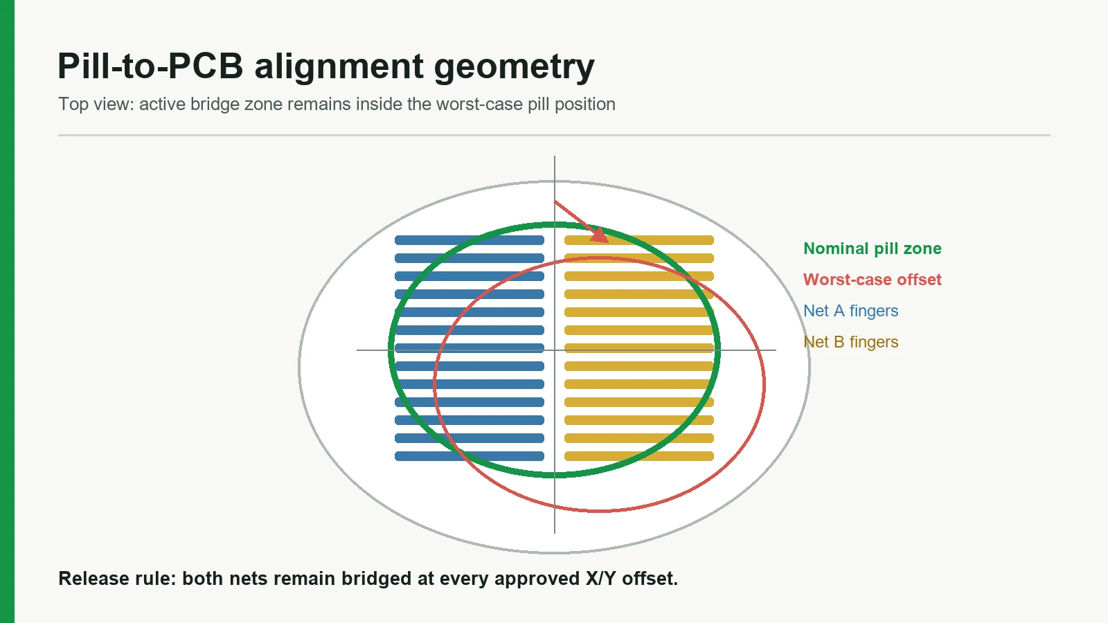
Size the active pattern from the finished pill and worst-case lateral offset, not a centered CAD view. Define:
- D_pill — maximum finished conductive diameter.
- D_pad — minimum usable diameter of the exposed two-net pattern.
- E_xy — maximum radial offset from molding, pill placement, locating clearance, housing/PCB registration, artwork, and key rock.
- M_edge — required functional margin beyond that offset.
For concentric circular envelopes:
D_pad ≥ D_pill + 2(E_xy + M_edge)
This is a conservative engineering calculation, not an IPC formula. Use arithmetic worst case unless a documented tolerance policy permits a statistical model.
| Carbon pill contact pattern | Useful condition | Main check |
|---|---|---|
| Parallel interdigitated comb | Solid round or rectangular pill | Offset across and along the fingers; finished trace/gap capability |
| Radial or fan fingers | Round pill with multidirectional offset | Narrow inner features, finish coverage, center routing |
| Annular interdigitated ring | Ring pill around an LED, vent, or opening | Inner/outer registration, rotational freedom, ring width |
| Opposed sectors or broad lands | Oriented oval or custom contact | Guaranteed overlap on both nets and local film sensitivity |
Northpoint publishes a 1.25:1 electrode-to-pill diameter as a supplier starting point. N&H separately advises a PCB contact dimension at least 0.5 mm larger than its keypad contact area. Neither is an IPC rule. Use these values only to challenge the project stack after the equation is solved. Northpoint guide and N&H guide.
The drawing needs three zones: a guaranteed pill zone at every approved offset, a functional bridge zone containing both nets, and a keep-out for adjacent nets, mask, legend, uncapped vias, component lands, and debris traps. Place keypad, housing, and PCB locating features on a common datum scheme. A larger pattern cannot repair uncontrolled assembly float or a hard stop that arrives before closure.
Use A/B Coupons When Geometry Is Still Open
Compare patterns without changing several variables at once. Hold pill lot and geometry, D_pad, PCB material, contact finish, fabrication lot, force/overtravel, excitation, fixture, and conditioning constant; vary only the comb, radial, annular, or sector topology. Test nominal registration and the approved X/Y corners, then repeat after the named residue or particle challenge. Record per-key resistance distributions and intermittent opens rather than a pass rate alone. If finish is the open decision, freeze one pattern and vary only the finish. This controlled comparison identifies whether geometry, coating, force, or contamination caused the observed change; a mixed coupon cannot. Complete it before final PCB release.
3. Choose the PCB Contact Finish by Duty
“Gold” is not a fabrication specification. ENIG, ENEPIG, electrodeposited engineering gold, and printed carbon use different processes and require different evidence.
| Contact surface | Public evidence | Release requirement |
|---|---|---|
| ENIG | IPC-4552B covers electroless nickel/thin immersion gold for contact use ; the gold cap is not impervious | Invoke the purchased revision; control thickness/corrosion evidence; qualify the real pill, motion, handling, and environment |
| ENEPIG | IPC-4556A covers nickel/palladium/immersion gold and includes soft-membrane and metallic-dome contact topics | Specify the full stack and verify the carbon-pill interface; listed use is not automatic approval |
| Electrodeposited engineering gold | ASTM B488-18(2025) covers purity, hardness, thickness, adhesion, and integrity; it excludes immersion gold | State type, hardness code, thickness, underplate, selective area, porosity/integrity, and keypad test |
| Screen-printed carbon | Ink and fabricator rules govern cure, film, sheet resistance, adhesion, overlap, and registration | Name the approved ink/equivalent, artwork layer, process controls, and assembled resistance test |
| Unqualified production finish | Solderability alone does not establish contact behavior | Record the deviation and test the matched interface before/after service-relevant exposure |
Use IPC-4552B, IPC-4556A, and ASTM B488-18(2025) within their scopes. Do not place “ENIG hard gold” on a fabrication drawing: ENIG uses immersion gold, while ASTM B488 applies to electrodeposited engineering gold and expressly excludes immersion coatings.
Printed carbon needs its own artwork. Eurocircuits publishes process-specific minima of 0.300 mm line width, 0.400 mm carbon-to-carbon spacing, 0.200 mm carbon-on-copper overlap, and 0.100 mm carbon-on-solder-mask overlap. These are Eurocircuits rules, not portable limits. They demonstrate why “carbon” cannot be a finish checkbox. Eurocircuits carbon-contact guide.
Before release, answer five questions: What stack is ordered? Which areas receive it? How is thickness or cured film verified? Which handling rule protects it? Which assembled-keypad test accepts it?
4. Specify the Pill, Compression, and Conductive Keypad Circuit Together
Abatek's contact-pill data conditions contact resistance on applied force. Closed resistance is therefore a force-conditioned assembly value, not a property of the conductive compound alone:
| Evidence layer | Named reference | What it can control | What it cannot establish alone |
|---|---|---|---|
| Conductive compound | ASTM D991-89(2026); ISO 1853:2018 | Bulk volume-resistivity method and material comparison | Pill-to-pad interfaces or complete switch resistance |
| PCB contact finish | IPC-4552B; IPC-4556A; ASTM B488-18(2025) | Finish family, process requirements, and coating controls | Performance with the selected pill, force, and contamination |
| Contact fixture | ASTM B539-20(2026)e1; ASTM B667-97(2024); IEC 60512-2-1:2002 | Excitation, probe/lead boundaries, and resistance method | Product life, enclosure effects, or circuit recognition |
| Installed circuit | IEC 60947-5-4:2002 + AMD1:2019; Texas Instruments TCA8418 | Electrical regime, thresholds, scan timing, debounce, and ghosting questions | Mechanical overlap, finish stability, or finished-product approval |
R_closed = R_trace A + R_interface A + R_pill + R_interface B + R_trace B + R_fixture
State whether fixture and trace resistance are included. Record excitation, sense points, two-wire or Kelvin method, force or travel, dwell, temperature, humidity, and conditioning.
initial pre-DV comparison input: R_closed ≤200 Ω for a new sample at the declared force/overtravel and low-level test condition. N&H publishes a sub-200-ohm carbon-pill entry. This is supplier reference data, an industry range, or a released limit. Replace it with the selected pill, finish, force window, circuit analysis, and conditioned evidence. N&H guide.
For an active-low input:
V_low = V_supply × (R_closed + R_series) / (R_pull-up + R_closed + R_series)
Worst-case V_low must remain below the guaranteed low-input threshold with noise margin. Include supply/pull-up tolerance, leakage, harness resistance, scan duty, temperature, and allowed drift. A matrix scanner adds row/column timing, debounce, simultaneous-key rules, and ghosting.
IEC 60512-2-1:2002 offers a millivolt-level connector method, and IEC 60947-5-4:2002 + AMD1:2019 addresses low-energy contacts. Either may inform an adapted fixture; neither certifies a silicone keypad. ASTM B667 likewise informs probe and connection boundaries, not a finished-keypad specification. Define first closure, measurement overtravel, hard-stop tolerance, center/edge presses, pill geometry, and open behavior on the same plan.
5. Treat Contamination Tolerance as a Test Condition
Contamination tolerance means a defined pill/pattern/finish/force stack still meets electrical acceptance after a named exposure. It is not implied by finger count, gold color, or pill diameter.
Residue, oil, dust, moisture, or finish change
→ fewer stable conducting spots
→ higher or intermittent interface resistance
→ the scanner misses its logic threshold
→ missed, repeated, or force-sensitive key response
ASTM B539-20(2026)e1 describes constriction and surface-film components of static contact resistance. It does not provide a universal contamination limit for a carbon-pill keypad.
Control four paths: PCB process residue; films transferred by molding, handling, adhesive, or lubricant; entry through bezel/vent/keypad edges; and real service fluids, cleaners, particles, humidity, and storage.
IPC-TM-650 2.3.28B can measure selected extractable ionic residues by ion chromatography. It does not prove the local pad is free of oil, mold release, or another organic film. Pair process data with assembled resistance, bounce, leakage, and functional scan. IPC-1601A separately treats contamination protection as a printed-board handling concern.
Low-molecular-weight siloxane remaining in silicone can volatilize and affect electrical contacts. This is a supplier/material-control question, not proof that every keypad has the problem or that one cure recipe solves it. Shin-Etsu KE-2017-50-A/B.
Do not prescribe a generic cleaning solvent. Confirm compatibility with the pill, silicone, carbon ink, finish, legends, adhesives, and housing; then challenge the complete stack with the actual contaminant.
6. Build an Electrical and Environmental Approval Matrix
A centered room-temperature continuity check is not design validation. Define sample quantity, severity, duration, powered state, recovery, and limits before testing.
| Gate | Controlled condition | Required record |
|---|---|---|
| Artwork/finish review | Datums, contact layers, mask, finish, fabricator coupon | Finished geometry, registration, finish evidence, revision |
| Baseline electrical map | Production-intent stack; declared excitation, force/overtravel, center and edge presses | Per-key closed resistance, leakage, intermittent opens, fixture ID |
| Force–travel–resistance | Slow press through closure and stop, then release | Closure travel, resistance versus travel, return, hysteresis |
| XY tolerance/circuit scan | Allowed offsets, supply corners, row/column timing, multi-key cases | Missed/false keys, V_low margin, bounce, ghost paths |
| Residue challenge | Named process residue, oil, dust, cleaner, or handling condition | Surface evidence plus resistance, leakage, intermittent events |
| Damp heat | Project-selected steady or cyclic humidity, powered state, recovery | Electrical/mechanical drift and visible condition |
| Temperature/fluid | Service profile, actual fluids, contact/wipe/rinse method | Closure at temperature, swelling/tack, finish or legend damage, recovery |
| Cycling/teardown | Declared rate, stroke, force, load, duty, interim reads | Serialized resistance and force/travel distributions, wear/film/datum findings |
IEC 60068-2-78:2025 covers steady damp heat without condensation. IEC 60068-2-14:2023 and IEC 60068-2-74:1999 provide temperature-change and fluid-contamination families. Standards do not choose the product severity.
Acceptance should state maximum resistance, allowed drift, leakage/open behavior, force/travel window, debounce assumption, edge-press rule, recovery, and failure handling. Keep raw serialized values and paired changes, not only a lot average.
Keep an Auditable Approval Record
Each serialized sample should connect the keypad lot, pill-material revision, mold/tool revision, PCB lot and fabricator, finish process, housing revision, assembly preload, firmware build, fixture ID, instrument ID, calibration status, operator, and test date. For every conditioning stage, retain baseline, during-exposure when required, recovered, and final values in the same units and at the same sense points.
The report should name the exact revision of every invoked method. ASTM F1578-24 addresses membrane-switch contact closure; use it for a molded-rubber keypad only as a project-approved, explicitly adapted reference. ISO 16750-4:2023 belongs only to road-vehicle programs. IEC 60068-2-78:2025, IEC 60068-2-30:2025, IEC 60068-2-14:2023, and IEC 60068-2-74:1999 provide environmental method families, but the project must select severities. Record every deviation instead of treating a modified method as standard compliance. Link electrical outliers to force–travel traces, scan captures, and teardown images.
See JASPER's testing and validation planning page as the required first-party quality link for this package. Regardless of supplier, component inspection does not approve the complete equipment.
7. Diagnose Contact Failures by Symptom
Change one part of the coupled stack at a time; a symptom is not a root cause.
| Symptom | Competing causes | Discriminating check |
|---|---|---|
| One key never closes | Missing pill, open net, offset, masked pad, inadequate travel | Cross-swap known-good PCB/keypad; net continuity; overlay; force–travel–resistance trace |
| Works only with high force | Late closure, early stop, surface film, pill shift, tight circuit limit | Controlled travel sweep before cleaning; center versus edge press |
| Center passes; edge fails | Key rock, weak datum, insufficient bridge zone, bezel/board deflection | Tolerance-corner build and slow oblique press with overlay |
| Humidity/fluid causes intermittency | Film, leakage, corrosion, swelling, trapped fluid | Paired pre/during/post electrical data and controlled recovery teardown |
| Double or missed presses | Bounce, brief opens, scan timing, debounce, ghost path, marginal V_low | Oscilloscope/logic capture synchronized to force/travel |
| Several keys drift together | Common finish/cleaning/compound lot, preload, connector, fixture error | Lot correlation, common-net test, reference resistor, keypad/PCB cross-swap |
| Resistance rises after cycling | Film growth, wear/transfer, force loss, datum shift, web damage | Serialized interval data followed by pad/pill inspection |
Cleaning may change a symptom without proving how a film formed. Capture evidence first. Correct geometry, finish, material, hard stop, circuit, firmware, or process only after the discriminating test identifies it.
8. When This Construction Is Not the Best Choice
An interdigitated PCB under a solid carbon pill is not the best choice when another requirement removes overlap margin or demands a different electrical regime.
- Center LED or opening: use an annular pill and ring pattern, or move the light path.
- Resistance below the qualified distribution of the selected carbon pill: evaluate a qualified low-resistance specialty pill, metal contact, metal dome, or discrete switch. Each has its own force/current/life conditions.
- Power or safety command: use a device and architecture rated for load, inrush, faults, redundancy, and the safety function. Do not infer this status from a signal contact.
- Thin printed interface: a membrane switch may fit better than a molded mat on rigid PCB. See JASPER's membrane keypad versus silicone keypad overview.
- No moving contact: capacitive touch may suit the interface, but glove/water behavior, EMC, false-touch rejection, haptics, and safety still need system validation.
Industrial, automotive, marine, outdoor, and medical uses remain conditional. Automotive parts need the program environment and change controls; marine/outdoor equipment needs enclosure testing; medical equipment must separate component manufacture from finished-device usability, cleaning, electrical safety, risk management, regulatory submission, and approval.
9. Release Package and Sample-Approval Checklist
Release one interface package with shared datums, circuit state, and acceptance revision.
| Package element | Required contents |
|---|---|
| Keypad | 2D/3D geometry; material; pill type/shape/size/tolerance; force/travel; web/plunger; vents; datums |
| PCB/FPC | Both contact nets; dimensions; mask/legend/via keep-outs; finish region; board datums; connector/netlist; fabrication evidence |
| Housing/stack | Retention, boss/hole fit, support, free gap, first closure, overtravel, hard stop, component keep-outs, worst-case section |
| Conductive keypad circuit | Supply/scan conditions, pull network, thresholds/leakage, simultaneous keys, debounce, ESD interface, fault response |
| Environment/process | Temperature, humidity, particles, fluids/cleaners, storage, packaging, handling, residues, wash limits |
| Approval/change control | Fixture, force/travel, dwell, excitation, sense points, samples, conditioning, limits, raw-data format, revalidation triggers |
Run the release in five moves: freeze the electrical detection window; freeze the pill drawing; overlay every tolerance corner; conduct joint DFM with molder, PCB fabricator, enclosure/electronics/assembly owners; approve production-intent samples and lock paired revisions. JASPER's PCB/FPC HMI assemblies page is the required integration link for this package.
Stop when the footprint predates the pill drawing, pad size lacks a datum overlay, “gold” or “carbon” is the whole finish note, resistance lacks force/excitation/conditioning, the hard stop can precede closure, or supplier changes can bypass regression testing.
JASPER's silicone keypad control-interface manufacturing case is the planned related-reading link, not independent evidence of a universal result.
10. Frequently Asked Questions
What is the best PCB contact pattern for a round carbon pill?
An interdigitated comb is a practical carbon pill contact pattern to evaluate first, but no footprint is universally best. Both nets must remain inside the guaranteed pill zone at every allowed offset and edge press. Compare comb, radial, or annular coupons when rock, center keep-out, contamination, or limited overlap drives the decision.
How much larger should silicone keypad PCB pads be than the pill?
Size silicone keypad PCB pads from maximum pill size plus twice the worst-case radial offset and required bridge margin. Northpoint's 1.25× ratio and N&H's 0.5 mm guidance are supplier starting points, not IPC rules. Release the dimension from actual molding, PCB, housing, and assembly tolerances.
Is ENIG the same as hard gold for rubber keypad contacts?
No. IPC-4552B defines ENIG as electroless nickel capped by thin immersion gold. ASTM B488 covers electrodeposited engineering gold by purity, hardness, thickness, adhesion, and integrity; it excludes immersion gold. Either finish still requires pill, force, wear, contamination, and conditioned-resistance validation.
What closed-contact resistance should a conductive keypad circuit accept?
Accept the highest resistance that preserves guaranteed logic margin across supply, pull resistance, leakage, series resistance, timing, and environmental corners. This article uses ≤200 Ω only as a source-backed pre-DV comparison input. It is not a standard or verified JASPER value and must be replaced before release.
How should contact resistance be measured?
Measure the complete net-to-net path on production-intent parts at declared force/overtravel, dwell, excitation, sense points, temperature, and conditioning. IEC 60512-2-1 may inform the method. Retain per-key distributions and intermittent events, not only a lot average.
How should contamination and humidity be tested?
Name the residue, dust, oil, cleaner, fluid, humidity mode, temperature, powered state, duration, and recovery. IPC-TM-650 can characterize selected ionic residues; IEC 60068-2-78 supplies a steady damp-heat framework. Repeat assembled resistance, leakage, bounce, scan, and visual checks.
Can a carbon pill switch a load directly?
Only when the selected contact system is expressly rated and validated for steady current, inrush, erosion, heating, duty, and faults. Carbon-pill keys often feed low-energy inputs, but product families differ. Use a rated switch, relay, or electronic interface when the load exceeds the validated regime.
What files are needed for a rubber keypad PCB contact design review?
Send the keypad drawing and pill geometry, PCB artwork/fabrication drawing, housing section, datum/tolerance stack, schematic and scan conditions, finish callout, environment/cleaning profile, and initial acceptance matrix. Put a revision on every file so keypad, PCB, housing, firmware, and test plan cannot drift independently.
11. Send the PCB Artwork and Pill Geometry
Before PCB release or keypad tooling, send the PCB artwork and pill geometry as one package with the housing stack, datums, finish, circuit thresholds, environment, cleaning process, and acceptance matrix. Request a marked-up worst-case overlay, unresolved assumptions, DFM questions, and production-intent test plan.
Submit the complete package through the engineering review route before PCB release or keypad tooling.
Technical References
- Source: IPC-4552B ENIG Specification. Accessed 2026.
- Source: IPC-4556 ENEPIG Specification. Accessed 2026.
- Source: N&H Technology Silicone Rubber Keypad Design Guide. Accessed 2026.
- Source: Shin-Etsu Conductive Silicone Rubber Technical Data. Accessed 2026.
- Source: IEC 60512-2-1 Contact Resistance Test Method. Accessed 2026.
- Source: IEC 60068 Environmental Testing Framework. Accessed 2026.
- Source: SparkFun's ring-contact construction. Accessed 2026.
- Source: ASTM D991-89(2026). Accessed 2026.
- Source: ISO 1853:2018. Accessed 2026.
- Source: ASTM B539-20(2026)e1. Accessed 2026.
- Source: Northpoint guide. Accessed 2026.
- Source: N&H guide. Accessed 2026.
- Source: IPC-4552B. Accessed 2026.
- Source: IPC-4556A. Accessed 2026.
- Source: ASTM B488-18(2025). Accessed 2026.
- Source: Eurocircuits carbon-contact guide. Accessed 2026.
- Source: Abatek's contact-pill data. Accessed 2026.
- Source: ASTM B667-97(2024). Accessed 2026.
- Source: IEC 60512-2-1:2002. Accessed 2026.
- Source: IEC 60947-5-4:2002 + AMD1:2019. Accessed 2026.
- Source: Texas Instruments TCA8418. Accessed 2026.
- Source: IPC-TM-650 2.3.28B. Accessed 2026.
- Source: IPC-1601A. Accessed 2026.
- Source: Shin-Etsu KE-2017-50-A/B. Accessed 2026.
- Source: IEC 60068-2-78:2025. Accessed 2026.
- Source: ASTM F1578-24. Accessed 2026.
- Source: ISO 16750-4:2023. Accessed 2026.
- Source: IEC 60068-2-30:2025. Accessed 2026.
Review the complete keypad stack before release
Send the keypad drawing, contact geometry, PCB artwork, environment, appearance targets, and validation plan for a project-specific review.