
For most high-use, conventionally shaped keys, a molded carbon pill is the lower-risk starting point among conductive rubber keypad contacts. It provides a substantial contact body, fixed geometry, and usually a wider process window. Printed carbon earns its place when the contact must be annular, irregular, broad, or too thin for a standard insert. Neither construction wins by name alone: contact force, PCB finish, finger pattern, contamination, and test method can reverse a paper comparison. Choose from samples of the complete keypad-and-PCB stack, not from an isolated material value.
JASPER certifications: ISO 9001, ISO 13485, IATF 16949, and ISO 14001.
1. Quick Decision: Which Contact Construction Fits the Key?
A carbon pill is the default for a round or oval contact that can be located securely in the mold. Printed carbon is the geometry tool. It can cover a ring around a light aperture or a custom footprint that would make pill placement awkward. The electrical decision remains conditional because Shin-Etsu Polymer publishes the same 20 Ω typical closed-contact resistance for its DCP printed contact and C40P molded pill when both are tested on the supplier's gold-plated PCB fixture.
| Decision dimension | Carbon pill usually leads | Printed carbon usually leads | Qualification required |
|---|---|---|---|
| Conventional round contact | ✓ | Confirm pill registration and overlap | |
| Annular or irregular contact | ✓ | Verify minimum print width and registration | |
| Low-profile deposited contact | ✓ | Validate compression and abrasion margin | |
| Lower resistance with standard carbon grades | ✓ | Not universal; compare on one PCB coupon | |
| Long actuation duty | ✓ | Supplier cycle figures use different endpoints | |
| Fewer post-molding electrical-process variables | ✓ | Pill placement remains a critical control | |
| Avoiding insert placement in restricted geometry | ✓ | Surface preparation, deposit, cure, and adhesion become critical | |
| Dirty or residue-prone enclosure | Neither contact removes the need for stack sealing and testing |
For an ordinary industrial key, begin with the pill and require the supplier to prove the final switch. Move to print when the mechanical drawing creates a specific geometric advantage—not simply because an ink datasheet shows a conductive value.
2. What the Two Silicone Keypad Contact Options Actually Are
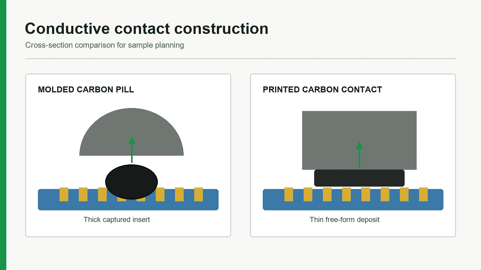
A molded carbon pill is a preformed piece of carbon-filled elastomer located at the underside of a silicone key. The keypad molding operation captures or co-molds the pill so that key travel presses it across two PCB conductors. Epec's manufacturing documentation shows conductive pills positioned in the mold before the silicone keypad is formed.
A printed carbon contact is a carbon-filled, silicone-compatible ink deposited on the underside of an already molded keypad. Silicone Dynamics describes it as an alternative where the geometry makes a conventional pill difficult to attach. This article uses “printed contact” only for ink on the rubber. Carbon printed over copper fingers on the PCB is a different design decision.
The contact is one layer in a switch stack. Each interface changes the result:
Operator finger
actuation force
key top / silicone web ← travel, snap, return force, overtravel
conductive contact ← pill diameter/thickness OR printed area/deposit
compression
interdigitated PCB pad ← overlap, finger width/gap, finish, cleanliness
sensing circuit ← pull-up/pull-down, debounce, threshold, test current
That stack explains why conductive rubber keypads cannot be specified by “carbon contact, 100 Ω” alone. A 4 mm contact arriving off-center, a web that bottoms before full compression, or residue on the PCB can dominate the bulk conductivity of the carbon compound.
A conductive keypad contact drawing therefore needs both mechanical and electrical datums. Locate the contact from the same features that locate the PCB; otherwise, independent keypad, housing, and board tolerances consume the overlap margin. State the free-state gap and available overtravel as well. A contact that just kisses the fingers may pass an unloaded continuity check yet never reach the stable resistance plateau seen at the intended actuation force.
Shin-Etsu's published geometries show the practical contrast. Its DCP printed carbon-silicone layer supports various 2.5–6.0 mm shapes at more than 0.03 mm thickness. Its C40P pill is round, 2.5–5.0 mm in diameter, and 0.55 mm thick. Those values describe two supplier products, not industry limits, but they make the tradeoff visible: print offers shape freedom; the pill supplies a thicker, discrete contact body.
3. How to Compare Conductive Rubber Keypad Contact Resistance
Three resistance units appear in contact literature, and they are not interchangeable.
| Quantity | Typical unit | What it measures | Appropriate use |
|---|---|---|---|
| Volume resistivity | Ω·cm or Ω·m | Electrical behavior through a material specimen | Compare compounds under a defined material test |
| Sheet resistance | Ω/square, sometimes normalized by thickness | Lateral resistance of a deposited film | Control conductive-ink formulation and deposit |
| Closed-switch resistance | Ω | Complete path across contact, PCB fingers, and interfaces | Approve the assembled keypad/PCB switch |
ASTM D991-89(2026) covers volume resistivity of electrically conductive and antistatic rubber. It does not predict the closed-switch value by itself. Creative Materials, for example, lists no more than 0.65 Ω·cm volume resistivity and no more than 250 Ω/sq/mil sheet resistance for its silicone-based 126-03(SP)C carbon ink. Those are material and film properties. They do not state what an assembled key will measure after pressing on a particular PCB.
Closed-switch resistance needs a fixture and operating point. IEC 60512-2-1:2002 defines a millivolt-level method for measuring resistance across mated contacts or between a contact and a gauge. IEC 60512-2-2:2003 addresses a specified-test-current method. These connector standards are useful method references; citing them does not make a rubber keypad an IEC-certified connector. A project still needs an agreed fixture, actuation force, circuit, dwell time, and limit.
Published values show why conditions matter
| Source and construction | Published contact value | Conditions disclosed near the value | What can safely be concluded |
|---|---|---|---|
| Shin-Etsu DCP printed carbon-silicone | 20 Ω typical; <200 Ω | Gold-plated PCB, 1.0 mm pitch, 0.5 mm track width; supplier method | This print system can equal the supplier's standard pill in one fixture |
| Shin-Etsu C40P standard pill | 20 Ω typical; <200 Ω | Same supplier gold-PCB fixture | Construction name alone does not determine resistance |
| Shin-Etsu Alpha97 low-resistance pill | 5 Ω typical; <20 Ω | Same supplier fixture | Compound grade can matter more than “pill versus print” |
| Abatek standard carbon pill | About 100 Ω | 1.5 N contact force | A representative pill benchmark, not a universal maximum |
| Abatek printed carbon ink | About 200 Ω | 1.5 N contact force | A representative printed-contact benchmark |
| N&H printed/dipped carbon | 150–300 Ω on gold; <600 Ω on carbon | Supplier guide and its pattern/test system | PCB contact finish changes the comparison |
| N&H standard pill | <100 Ω on gold; <200 Ω on carbon | Same guide context | Pill commonly offers more margin in this supplier system |
These values should not be averaged into one “industry resistance.” The sources use different compounds, areas, forces, finishes, traces, and endpoints. They do support one procurement rule: compare both constructions at the same contact force on the same production-representative PCB coupon.
Use <=200 ohms at 1.5 N as the first sample-screening limit. Record the PCB finish, pattern, test current or voltage, conditioning, sample count, and whether the limit applies at incoming, conditioned, or end-of-life inspection. Release the drawing limit from the verified project distribution and circuit margin.
4. Geometry, Attachment, and the PCB Pattern
Geometry often settles the carbon pill vs printed contact decision before electrical testing begins. A round pill is easy to dimension, locate, inspect, and match to a symmetric PCB pattern. A printed contact can follow an annulus around an LED, fill an elongated key, or cover an area where a 0.55 mm insert would upset the stack height.
The two constructions fail registration in different ways. A pill can shift in its mold location, tilt, sit proud, or lose effective overlap after keypad-to-PCB assembly tolerances accumulate. A print can have edge loss, pinholes, thickness variation, or X-Y registration error. Printing removes an insert-placement problem but adds a deposited-film process.
A contact-pattern drawing must close the tolerance loop
The active PCB area should remain under the conductive contact at the worst permissible keypad, housing, and PCB offsets. Extend the PCB contact area at least 0.5 mm beyond the keypad contact in each direction and shows a 0.3 mm trace / 0.3 mm spacing test comb. Diamond HMI offers a different supplier starting point: a pad at least 1.25 times the pill size, 0.5 mm interdigitated fingers, and a 0.6 mm gap. Neither is an international standard.
Use those dimensions to start a review, then calculate the actual stack:
| Drawing input | Carbon-pill question | Printed-contact question |
|---|---|---|
| Contact outline | Is a standard round/oval size available? | Is every neck or ring wide enough to print repeatably? |
| X-Y tolerance | Does the pill retain required finger overlap at worst case? | Does print-to-mold registration retain required overlap? |
| Contact height | Does the pill touch only after the designed travel? | Does the thinner deposit still achieve full compression/contact? |
| PCB finger pattern | Are enough parallel shorting paths covered? | Does the entire printed shape bridge both nets without marginal edges? |
| Surface finish | Is the selected finish compatible with resistance and wear targets? | Was the ink/finish pair tested rather than assumed? |
| Vent path | Can trapped air or vacuum oppose key travel? | Can the printed region or sealing land block the intended vent? |
Gold over nickel is common in supplier guides for high-reliability contact coupons, but the article does not prescribe one universal finish. The chosen finish, finger geometry, and conductive contact must be sampled together. If the circuit uses a carbon-coated PCB contact, do not import a resistance value measured on gold.
5. Wear, Contamination, and the Failure Chain
A molded pill is generally the safer starting point for frequent actuation because its conductive body is much thicker than a printed film. N&H's guide lists 1–3 million operations for its printed/dipped category and more than 5 million for standard pills. Diamond HMI describes printed carbon around 10–20 μm thick. These figures are design-guide benchmarks, not a universal life claim: the sources do not share one load, stroke, environment, resistance endpoint, or failure definition.
Printed carbon is therefore not automatically a short-life choice. Shin-Etsu publishes equivalent initial electrical ratings for its DCP print and C40P pill, but does not publish a separate DCP-versus-C40P electrical endurance comparison on that page. The honest test is the production construction under the project duty cycle.
Failure chain: inspect causes before blaming the carbon grade
| Cause | Physical change | Likely electrical symptom | Verification or control |
|---|---|---|---|
| Pill or print misregistration | Reduced overlap with PCB fingers | High or force-sensitive resistance; intermittent closure | Optical X-Y measurement plus worst-case stack overlay |
| Incomplete key compression | Contact touches only part of the pattern | Resistance falls sharply as force increases | Resistance-versus-force curve and housing stop review |
| Dust, lint, or dried residue | Insulating film at the interface | Higher resistance, bounce, or open circuit | Clean/contaminated coupon comparison; enclosure and sealing review |
| Printed-film abrasion | Local thinning or loss of conductive path | Rising resistance or intermittent contact | Microscopy and resistance checkpoints during endurance |
| Printed-film crack or adhesion loss | Discontinuous film or lifted edge | Unstable/open contact | Bend/compression conditioning plus adhesion inspection |
| Pill surface wear or glazing | Changed real contact area | Resistance drift | Surface inspection and end-of-life resistance distribution |
| PCB finish wear or oxidation | Less stable finger interface | Drift, bounce, force sensitivity | Coupon finish verification and post-test microscopy |
| Ink mix or cure variation | Filler distribution or polymer network changes | Lot-to-lot resistance/adhesion shift | Mix time, viscosity, deposit, oven profile, and coupon controls |
Paul Knupke's Epec paper ties nonconductive contamination at the pill/PCB interface to increased resistance, greater switch bounce, and an open switch. That mechanism applies to both constructions because both expose a carbon surface to the PCB. A thicker pill does not seal an enclosure, and a printed contact does not remove residue sensitivity.
The sensing circuit also needs margin. If firmware recognizes only a near-zero closure, a contact can fail functionally while remaining mechanically intact. The electrical team should set a recognition threshold above the approved end-of-life resistance distribution, then verify debounce behavior with the real scan rate and pull-up/pull-down network.
6. Process Controls That Separate a Prototype from a Repeatable Part
Carbon pills and printed contacts shift risk to different manufacturing steps. The useful question is not which process has fewer steps; it is which critical variables the supplier can measure and hold.
| Control stage | Carbon pill | Printed carbon contact |
|---|---|---|
| Incoming material | Compound grade, pill dimensions, resistivity/lot identity | Ink identity, shelf life, storage, viscosity, filler dispersion |
| Placement / application | Cavity presence, orientation, X-Y location, retention | Surface preparation, fixture, stencil/screen condition, registration |
| Geometry | Diameter, thickness, flatness, molded exposure | Wet/dry deposit, edge definition, pinholes, minimum feature width |
| Thermal process | Silicone molding and post-cure effect on pill/key bond | Ink cure time, part temperature, airflow, oven loading |
| In-process evidence | Vision check, dimensional sampling, resistance coupon | Viscosity log, deposit measurement, cure profile, adhesion coupon |
| Final evidence | Resistance distribution at defined force | Resistance distribution plus film/adhesion inspection |
Creative Materials supplies 126-03(SP)C ready to use at 40,000 cP, instructs processors to re-suspend settled carbon filler, and recommends 60 minutes at 150°C for good properties while telling users to establish the optimum process for the actual substrate. That is a useful example of the controls a print process may need. It is not a qualified JASPER ink or cure recipe.
A printed sample can look black and continuous while missing its electrical or adhesion target. A pill can look correctly molded while sitting outside the intended PCB overlap. For both, inspection must measure the characteristic that closes the switch: registered area, surface condition, compression, and resistance on a representative PCB.
Process capability should follow sample approval. Once dimensions and test conditions are frozen, review distributions by cavity, key position, ink or pill lot, and production run. A single “golden sample” cannot show lot-to-lot drift or a cavity-specific placement error.
7. Sample Approval Test Matrix
Sample testing should isolate material, process, and stack effects without pretending they are the same measurement. Use material coupons to monitor compound or ink. Use assembled keypad/PCB fixtures to approve switch behavior.
| Stage | Samples / condition | Measurements | Decision purpose |
|---|---|---|---|
| Incoming baseline | Multiple keys across mold cavities and keypad locations | Contact outline, X-Y registration, pill thickness or dry print deposit, visual defects | Detect placement, print, or cavity bias |
| Force sweep | Same key measured from first closure through intended overtravel | Closed-switch resistance versus force; closure force; return behavior | Show whether housing travel reaches a stable contact plateau |
| PCB comparison | Same contact construction on agreed production finish; optional controlled alternate coupon | Resistance distribution and bounce at one force/current | Separate PCB-finish/pattern effect from rubber construction |
| Environmental conditioning | Project-specific temperature/humidity/chemical exposures, defined from the end use | Resistance before/after recovery; visual and adhesion inspection | Detect moisture, residue, swelling, oxidation, or adhesion sensitivity |
| Contamination challenge | Defined dust or residue only when relevant and safely reproducible | Resistance, bounce, recovery after approved cleaning | Verify enclosure/cleanliness margin rather than claim immunity |
| Mechanical endurance | Representative force, stroke, rate, dwell, alignment, and electrical load | Resistance and force at planned checkpoints; surface microscopy | Establish drift and failure mode, not just “cycles survived” |
| End-of-life functional test | Aged keypad in the actual housing and electronics | Recognition margin, debounce, stuck/open behavior | Prove the system accepts the contact distribution |
For low-disturbance baseline resistance, an IEC 60512-2-1-style millivolt method can inform fixture design. If the production circuit applies a defined current, IEC 60512-2-2 provides a specified-current measurement reference. IEC 60512-2-3 covers resistance variation under dynamic conditions and can inform a bounce or movement study. The drawing must still state the project method because these standards were not written specifically as a complete rubber-keypad qualification specification.
Record the conditions beside every resistance result
A defensible test record includes:
- contact construction, material/ink grade, dimensions, and lot;
- key position and mold cavity where traceable;
- PCB material, finish, finger width/gap, and active area;
- applied force, travel or overtravel, fixture alignment, and dwell;
- test voltage/current, instrument method, and sampling rate;
- temperature, humidity, preconditioning, and recovery time;
- sample count, checkpoints, pass limit, and raw distribution;
- failure definition: resistance, intermittency, bounce, adhesion, force loss, or physical damage.
The <=200 ohms at 1.5 N screen keeps early comparisons consistent. The production drawing must carry the verified project limit and the complete measurement conditions. JASPER's keypad testing and validation page defines the evidence package for that release.
8. Carbon Pill vs Printed Contact Decision Matrix
The right choice follows the dominant risk in the drawing and circuit.
| If the project priority is… | Start with… | Why / required proof |
|---|---|---|
| Conventional round key with frequent use | Carbon pill | Mature geometry and substantial contact body; prove resistance and overlap |
| Annular contact around a light opening | Printed carbon | A print can form the ring; prove minimum width, registration, and uniform deposit |
| Irregular or broad footprint | Printed carbon | Avoids forcing a standard pill into unsuitable geometry; validate edge coverage |
| Lower standard-carbon resistance margin | Carbon pill | Supplier guides commonly show lower limits; compare on the production PCB |
| Very low or tightly stable resistance | Neither standard option by default | Evaluate a qualified low-resistance pill, plated contact, metal dome, or discrete switch |
| Harsh contamination exposure | Neither without enclosure work | Improve sealing/cleanliness and test the assembled stack |
| Supplier cannot document ink preparation and cure | Carbon pill, if geometry permits | Uncontrolled deposit and cure make print approval weak |
| Supplier cannot hold pill placement | Printed contact, if its process is controlled | Printing may remove insert-placement risk but adds adhesion/deposit controls |
| Key only actuates a separate switch | Nonconductive actuator | The silicone need not carry the electrical contact; consider PCB switch or membrane switches |
A recommendation to use a pill is not the best choice when its standard shape compromises lighting, overlap, or package height. A recommendation to print is not the best choice when the supplier cannot demonstrate adhesion and resistance stability through the specified duty cycle.
9. Drawing and Sample-Approval Checklist
Before choosing the conductive keypad contact, place these inputs in the drawing package or engineering RFQ:
- [ ] Contact construction named: standard pill, low-resistance pill, or printed-on-silicone carbon.
- [ ] Contact outline, thickness/deposit, location, and X-Y tolerances.
- [ ] Silicone grade, hardness, web geometry, force, travel, snap ratio, and overtravel stop.
- [ ] PCB finish, interdigitated pattern, active area, venting, and assembly datum.
- [ ] Closed-switch resistance limit with force, current/voltage, dwell, and fixture.
- [ ] Initial, conditioned, and end-of-life acceptance limits.
- [ ] Environmental exposures, cleanliness level, and enclosure/sealing assumptions.
- [ ] Endurance force, stroke, rate, cycles, electrical load, and failure definition.
- [ ] Print controls: surface preparation, ink identity, deposit, cure, and adhesion test.
- [ ] Pill controls: grade, dimensions, placement, retention, and cavity sampling.
- [ ] Raw-data and traceability requirements for sample approval.
The broader silicone rubber keypad materials and contact options should be frozen with the contact decision, not afterward. To choose the construction, send JASPER the keypad section, PCB contact artwork, circuit threshold, and validation conditions through the engineering contact page. Any supplier recommendation should remain initial until both constructions are tested on the intended stack.
10. Frequently Asked Questions
What is the difference between a carbon pill and a printed contact in a rubber keypad?
A carbon pill is a preformed conductive elastomer insert captured in the silicone keypad. A printed contact is a thin carbon-filled ink deposited on the molded key underside. The pill favors standard geometry and a substantial contact body; print favors irregular, annular, broad, or low-profile geometry.
Which conductive keypad contact has lower resistance?
A standard carbon pill often provides more resistance margin, but not always. Shin-Etsu lists 20 Ω typical and less than 200 Ω for both its DCP printed contact and C40P pill on the same gold-PCB fixture. Compare production candidates at equal force on one PCB coupon.
Can printed carbon make a ring around an LED or light guide?
Yes. Abatek identifies free-form printed carbon geometries, including a ring around a lighting area. The drawing still needs a minimum ring width, print-to-mold registration tolerance, PCB overlap, vent path, and evidence that the cured film remains conductive and adhered after conditioning.
Does a larger carbon pill always reduce contact resistance?
No. A larger pill may cover more parallel PCB fingers, but material grade, flatness, contact force, finger pattern, finish, alignment, and contamination also control the measured resistance. Abatek publishes different limits by pill diameter, which supports treating area as one variable rather than a guarantee.
Which PCB finish works with conductive rubber keypad contacts?
Gold-over-nickel and carbon contact surfaces both appear in supplier guides, but they produce different resistance results. N&H reports separate values for gold and carbon PCB contacts. Specify the actual finish and test the selected pill or print on production-representative finger geometry.
How should contact resistance be measured on keypad samples?
Measure the assembled keypad against a defined PCB coupon at a stated force, travel, current or voltage, and environment. Record the full resistance distribution. IEC 60512-2-1 and -2-2 can inform low-level or specified-current methods, but the project must define its own fixture and limits.
Are carbon pills always more durable than printed contacts?
No universal life ratio is defensible. Supplier guides commonly assign longer cycle benchmarks to molded pills, yet the endpoints and conditions differ. Approve durability using the intended force, stroke, alignment, PCB finish, environment, electrical load, inspection checkpoints, and resistance-failure definition.
When should an engineer choose neither construction?
Choose neither standard carbon option when the circuit needs a much lower or more stable interface than samples can prove, when contamination cannot be controlled, or when the silicone key only needs to actuate another switch. Evaluate a qualified low-resistance pill, plated contact, metal dome, or discrete PCB switch.
11. Material Compliance Evidence
Material declarations must be tied to the actual part construction, supplier records, regulation version, and applicable exemptions.
Material compliance evidence
| Evidence category | Required record | Acceptable wording boundary |
|---|---|---|
| Product-applicable RoHS, REACH, or other requested material declarations | Current supplier declarations or test reports, covered materials and part numbers, regulation/version, exemptions, date, and responsible approver | State applicability to the named material or part; do not convert a declaration into a product certification |
Technical References
- Source: Shin-Etsu Conductive Silicone Rubber EC Series. Accessed 2026.
- Source: N&H Technology Silicone Rubber Keypad Design Guide. Accessed 2026.
- Source: Abatek Silicone Keypad Design Guide. Accessed 2026.
- Source: IEC 60512-2-1 Contact Resistance Test Method. Accessed 2026.
- Source: ASTM D991 Conductive Rubber Volume Resistivity. Accessed 2026.
- Source: Tektronix and Keithley Low Level Measurements Handbook. Accessed 2026.
- Source: Shin-Etsu Polymer Europe, “Contact element for keypads”. Accessed 2026.
- Source: Epec Engineered Technologies, “Rubber Keypad Manufacturing Process”. Accessed 2026.
- Source: Silicone Dynamics, “Carbon Contact Ink”. Accessed 2026.
- Source: ASTM D991-89(2026), “Rubber Property—Volume Resistivity of Electrically Conductive and Antistatic Products”. Accessed 2026.
- Source: Creative Materials, 126-03(SP)C datasheet, revision July 15, 2019. Accessed 2026.
- Source: IEC 60512-2-1:2002, Test 2a. Accessed 2026.
- Source: IEC 60512-2-2:2003, Test 2b. Accessed 2026.
- Source: Abatek, “Contact Technology”. Accessed 2026.
- Source: N&H Technology, “Silicone Rubber Keypad Design Guide”. Accessed 2026.
- Source: Diamond HMI, “Rubber Keypad Design Guide 2021”. Accessed 2026.
- Source: Paul Knupke, Epec, “High Reliability Keypads: Design Factors That Affect Performance”. Accessed 2026.
- Source: IEC 60512-2-3:2002, Test 2c. Accessed 2026.
- Source: Abatek, “Silicone Keypad / Contact Pills”. Accessed 2026.
Review the complete keypad stack before release
Send the keypad drawing, contact geometry, PCB artwork, environment, appearance targets, and validation plan for a project-specific review.