
Choosing capacitive touch cover lens thickness means balancing mechanical protection against usable touch margin in the complete assembly. There is no universal maximum: material permittivity, coatings, printed ink, adhesive, air gaps, electrode pitch, controller range, gloves, water, display noise, grounding, and production variation all change the result. An OEM should compare production-intent stacks, then approve the thinnest construction that meets the mechanical requirement—or a thicker construction only after the selected sensor and controller demonstrate the required inputs and reject invalid ones in the installed equipment.
JASPER certifications: ISO 9001, ISO 13485, IATF 16949, and ISO 14001.
A nominal value such as “2 mm glass” is a sourcing input, not a touch specification. The operator couples through every layer above the electrodes, while conductors behind and beside the sensor shape the field. For display products, the review should include the cover, sensor, bond, display, bezel, FPC, controller, firmware, power and enclosure. JASPER is one manufacturer an OEM can ask to review touch panels with display windows; the proposal still needs to state who owns sensor design, tuning, display integration and final-equipment validation.
1. Why Nominal Capacitive Sensor Cover Thickness Is Not Enough
The electrical question is not simply “How thick is the glass?” It is “Can the selected electrode/controller system distinguish the weakest approved touch from noise and invalid objects through the released dielectric stack?” Thickness affects that answer, but so do relative permittivity, electrode area and pitch, local gaps, nearby conductors and controller signal-to-noise margin.
Texas Instruments uses the familiar first-order relationship:
C = εr × ε0 × A / d
where:
C = capacitance
εr = relative permittivity of the dielectric
ε0 = permittivity of free space
A = effective coupled area
d = separation through the dielectric
The TI CapTIvate Design Guide presents this relationship as part of capacitive-sensor design and lists representative relative permittivity values of 1.0 for air, 2.8 for acrylic, 2.9–3.0 for polycarbonate and 7.6–8.0 for glass. Those figures explain direction, not finished-panel performance. PCAP electrodes produce fringing fields rather than an ideal parallel-plate field, and actual material grades, finite electrode geometry and parasitic capacitance matter.
For comparing layered concepts, engineers can use a screening quantity:
effective dielectric distance ≈ Σ (layer thickness ti / relative permittivity εri)
A lower total generally supports stronger coupling when the electrode geometry and other conditions stay fixed. The model is useful for finding obvious stack penalties. It is not a controller-tuning equation or a substitute for measurement.
| Example layer, using TI representative εr | Physical thickness used for comparison | Approx. t/εr contribution | What the comparison shows |
|---|---|---|---|
| Air | 0.10 mm | 0.100 mm | A small uncontrolled void can consume substantial effective dielectric distance |
| Glass | 1.00 mm | 0.125–0.132 mm | Higher representative εr reduces the first-order penalty per physical millimetre |
| Polycarbonate | 1.00 mm | 0.333–0.345 mm | Grade and hardcoat still need actual material data and testing |
| Acrylic / PMMA | 1.00 mm | 0.357 mm | Mechanical, optical and chemical requirements remain separate decisions |
The table does not prove that 1 mm glass always outperforms 1 mm plastic. It isolates one electrical term. A glass panel may include a thicker black mask, a different adhesive, a larger display gap or a metal bezel. A plastic lens may permit closer electrodes, shaped geometry or a different support. Actual permittivity can also vary with formulation, frequency, temperature and moisture.
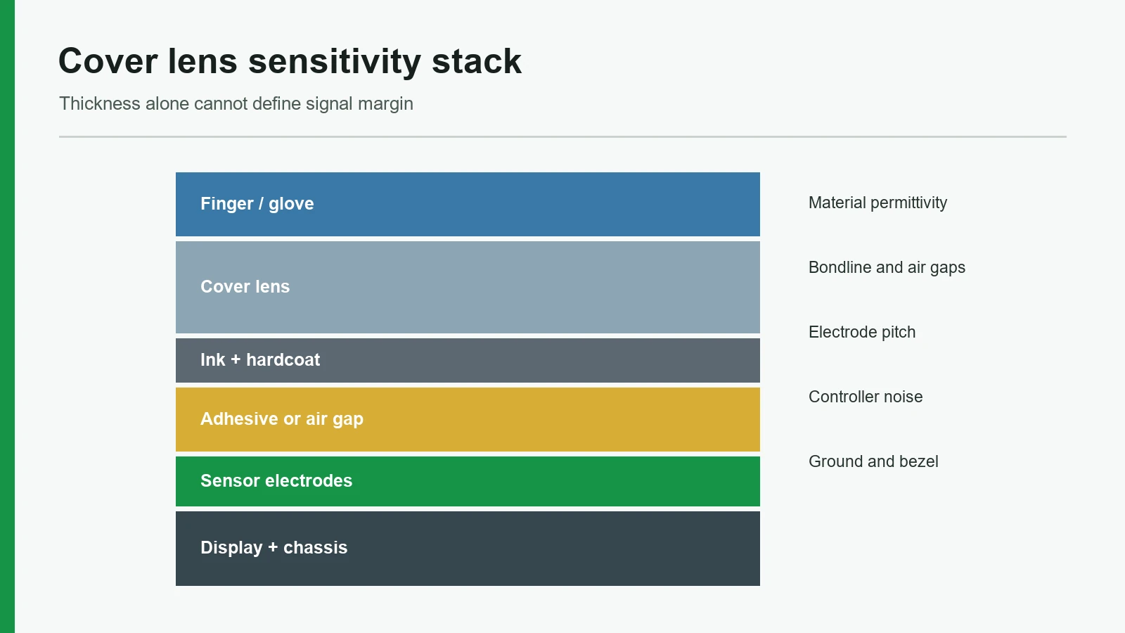
The production stack should therefore be drawn in full:
Approved finger / glove / conductive stylus / unintended object
v
Surface coating, texture, contamination and moisture
v
Cover lens: glass, PMMA/acrylic or polycarbonate
v
Clear area / black mask / dead-front ink / metallic decoration
v
OCA, LOCA, PSA, perimeter bond or intentional air gap
v
Sensor substrate + Tx/Rx or discrete electrodes + edge routing
v
Display gap / optical bond + display + bezel + chassis + ground
v
FPC + controller + configuration + host software
The useful drawing is not one stack in the centre. It includes centre, edge, corner, printed-border, adhesive-transition and bezel sections because local construction can differ.
2. How to Specify Capacitive Touch Cover Lens Thickness: Eight Design Gates
A defensible selection passes eight gates. Each gate produces a drawing, data field or test record. If one remains open, a successful bench tap should not release the lens.
| Gate | Acceptance evidence | Release blocker |
|---|---|---|
| 1. Complete stack | Every layer has a material, nominal, tolerance, coverage and revision | The RFQ says only “3 mm cover glass” |
| 2. Material | Electrical, mechanical, optical, chemical and process requirements are separated | Glass, PMMA and polycarbonate are treated as interchangeable |
| 3. Bond or gap | Adhesive/gap geometry, ink step, support and void criteria are intentional | Temporary tape or uncontrolled bubbles represent production |
| 4. Local border stack | Clear, printed, metallic, dead-front and bezel zones are mapped | A centre test approves the whole panel |
| 5. Electrode/controller pair | Pitch, pattern, edge cells, routing and controller are reviewed with the final cover | A generic sensor is frozen first |
| 6. Use states and noise | Weak valid inputs and strong invalid/noise states are named and measured | “Increase sensitivity” is the requirement |
| 7. Mechanical objective | Impact/support goals and sensing margin are tested separately | More thickness is assumed to solve durability without side effects |
| 8. Release control | Sample IDs bind hardware, firmware, enclosure, method and result | One unlabeled golden sample releases production |
Gate 1 — Freeze every layer between the operator and the electrodes
Start with a section drawing, not a material name. Record the surface coating, cover grade, nominal thickness and tolerance, curvature or flatness, printed layers, adhesive product and coverage, local gap, sensor substrate, electrode plane and rear support. If the display is bonded to the touch sensor or separated by an air gap, include that interface too.
Texas Instruments identifies overlays, labels, inks, adhesives, transition materials and air gaps as capacitive design inputs. Microchip’s AN2934 Capacitive Touch Sensor Design Guide likewise connects cover thickness with field spread, contact size, electrode geometry, shielding and nearby conductors. Neither source supports approving a lens by nominal thickness alone.
Tolerances belong in the model. A 2.0 mm nominal cover, for example, must be evaluated at the maximum released lens thickness, maximum bondline and worst allowed local step—not only at nominal. The weakest valid input may occur at one tolerance extreme, while false response to water or noise may appear at another.
the stack drawing uses material codes, nominal/tolerance, coverage maps and common datums for the cover, print, bond and sensor.
a clear unprinted coupon passes, then production adds coating, black mask and a different adhesive without electrical review.
Gate 2 — Choose the cover material by requirements, not dielectric constant alone
Material permittivity affects coupling, but the cover also carries loads, presents the visible surface and must survive the actual cleaning and environment. A useful selection table keeps these decisions separate.
| Cover route | Reasons to consider it | Questions before release | When it may be the wrong choice |
|---|---|---|---|
| Strengthened glass | Rigid optical front, hard surface, second-surface printing, established display integration | Glass composition, strengthening route, edge/holes, thickness tolerance, flatness, impact/support target, coating, print and bond stress | Weight, edge vulnerability, shaped geometry, field service or certain impact modes dominate |
| PMMA / acrylic | Machining, optical clarity, lower mass and shaped/plastic-front options | Grade, hardcoat, scratch target, chemical list, UV/thermal exposure, flatness, print and adhesive compatibility | Solvents, abrasion, temperature or creep exceed the qualified construction |
| Polycarbonate | Impact-oriented plastic cover and formed geometry options | Grade, hardcoat, chemical stress cracking, optical requirement, temperature, print, support and dimensional stability | Surface durability, chemical exposure or optical stability cannot be controlled |
| Hybrid supported front | Thin decorated face over a separate structural support | Support flatness, bond continuity, local gaps, edge seal, assembly sequence and service method | The multiple interfaces create more variation than the architecture can tolerate |
TOPPAN publishes one cover-glass example range of 0.7–3.0 mm in soda-lime or aluminosilicate glass with clear or anti-glare surfaces and optional anti-reflective or anti-fingerprint treatment. That range shows available sourcing choices; it is not a sensitivity range or a JASPER capability. The selected thickness still comes from the product’s mechanical analysis and measured touch margin.
Decorative and structural glass also need different language. JASPER’s glass nameplates route is relevant when reviewing glass finish, print and visible features. A decorative-glass capability does not by itself establish PCAP sensor compatibility. The touch drawing must bind the exact glass and decoration to the sensor stack.
the material specification states what mechanical, optical, chemical and electrical evidence chooses the grade.
a higher dielectric constant is used to claim better touch performance while edge support, coating, print, bond and controller remain undefined.
Gate 3 — Treat optical bonding and air gaps as electrical geometry
Touch sensitivity through glass depends strongly on what sits beneath the glass. A continuous, qualified optical adhesive can remove an uncontrolled air interface and stabilize sensor-to-cover spacing. It can also introduce bondline tolerance, ink-step coverage, stress, bubble, particle, cure, aging and rework requirements. A perimeter bond or intentional air gap can preserve modular service and reduce full-area lamination complexity, but the gap must be dimensioned and supported.
3M’s OCA 8211–8215 data sheet lists 25, 50, 76, 100 and 125 µm products in that named family. A separate 3M CEF28XX/OCA 802XX family lists 100–350 µm nominal options and links step coverage to conformability. These are material examples—not approval to select 100 µm, 250 µm or any other bondline by blog rule. Ink height, substrate flatness, pressure, temperature, vacuum/autoclave process where applicable and adhesive rheology decide whether a local step can be filled.
An air gap deserves the same control. The first-order table shows why 0.10 mm of air can contribute a dielectric distance comparable to much thicker glass. The real effect also depends on the sensor field and whether the void is local, continuous or moving under pressure. A variable bubble or edge lift is not the same as a dimensioned display air gap.
Full optical bonding is not automatically the best construction. A serviceable industrial display may favor a replaceable perimeter-bonded module. A large panel with uncertain flatness may need a different material or process route. The chosen architecture wins only when optics, sensing, stress, sealing, rework and production controls fit the equipment.
the drawing names adhesive, thickness/tolerance, coverage, print-step profile, surface preparation, support, void/cosmetic criteria and process owner.
“optically bonded” is treated as a performance specification with no product code, process window or sample evidence.
Gate 4 — Map black masks, dead-front inks and metallic decoration
PCAP cover lens design changes at the border. The clear display area may have only coating, glass and adhesive. The surrounding black mask can contain several printed passes. Dead-front icons add local optical density. Metallic or conductive decoration can reshape the electric field. The adhesive may terminate near that step, while the bezel or chassis approaches from behind.
Create at least four cross-sections when applicable:
- Clear viewing area over the sensor and display;
- Printed black-mask area over edge electrodes;
- Adhesive transition or perimeter-bond edge;
- Bezel, gasket, frame, fastener or chassis approach.
Control print layer order, cured thickness profile where critical, color/optical criteria, window registration, conductive-material restrictions and lit/unlit inspection. Metallic decoration should not be substituted by appearance alone. A pigment, coating or ink supplier change can be an electrical change even if color remains within tolerance.
Edge targets deserve separate tests because electrode termination, routing density, ground/chassis proximity and local dielectric thickness differ from the centre. IEC 62908-12-10:2025 recognizes centre and edge regions in touch-performance measurement. The project must still choose its probe, edge width, points, operating states and acceptance limits.
artwork, stack sections and sensor overlays share one datum and identify local electrical risks.
the approval report contains centre taps only, while the production UI places critical controls in the printed border.
Gate 5 — Pair electrode pitch and controller range with the real cover
A thicker cover changes field distribution and reduces the touch-induced signal seen by the selected architecture. Infineon’s cover-glass thickness and sensor pitch require balance. Microchip AN2934 gives 4–10 mm pitch with 6 mm typical for named mutual-capacitance surface-pattern examples. Those numbers are not a universal answer; they show why the cover and electrode drawing must be developed together.
Larger pitch or electrode area can increase interaction with a finger through some covers, but it can reduce spatial resolution, alter edge behavior, increase parasitic loading or constrain small targets. A coordinate PCAP display, a discrete capacitive key and a slider do not share one optimum pattern. The controller’s acquisition method, channel count, analog range, scan frequencies, filters, shield support and diagnostics also matter.
Freeze these items as one revision set:
- cover and complete dielectric stack;
- sensor architecture, pattern family, pitch/gap and edge termination;
- Tx/Rx or channel map, border routing, FPC and connector;
- controller device/family and hardware revision;
- configuration, firmware and host mapping;
- raw-data or diagnostic method;
- display, ground, shield, bezel and enclosure state.
The related capacitive multi-touch electrode pattern design guide covers pitch, routing and edge geometry in more detail. Its final route is retained even if the page is not yet live.
feasibility samples use the intended controller, sensor artwork and maximum production-intent stack.
a sensor is purchased from a standard catalog, then firmware is expected to compensate for any glass, glove, display or bezel later.
Gate 6 — Define sensitivity as decision margin across real use states
“High sensitivity” is not a pass criterion. The controller must separate the weakest valid touch from the strongest invalid change caused by noise, water, baseline movement, assembly variation and unintended objects.
usable decision margin
= weakest approved valid response
− strongest combined invalid response and variation
This is a review model, not a controller equation. Lowering a threshold may recover a dry glove and admit droplets, a sleeve, display noise or an adjacent target. Raising gain can amplify useful signal and unwanted variation. Filtering can reduce noise and add latency or slow release. Geometry, stack, grounding and state logic may need correction before another firmware adjustment.
Specify the input article: bare finger, conductive stylus if allowed, glove manufacturer/model/material/size/layers/fit, wet condition and target geometry. Specify invalid states too: palm, sleeve, nonconductive tool, condensation, droplets, cleaning wipe, pooled liquid and an inactive border. Record display brightness/refresh, charger or motor states, radios, power transitions and temperature conditions capable of changing noise.
The capacitive touch water and glove tuning guide provides a state-based method. It does not supply a universal glove thickness or wet-mode setting.
raw or diagnostic data compare the weakest approved input with the strongest invalid/noise state on identified assemblies.
one dry centre tap at room conditions is labeled “works through 5 mm glass.”
Gate 7 — Separate impact protection from touch feasibility
A thicker cover can support a mechanical protection objective, but thickness alone does not establish impact performance. Glass type, strengthening, edge condition, holes, unsupported span, mounting, adhesive/gasket, preload, enclosure stiffness, impactor and test method all matter. A touch supplier should not convert one ball-drop or impact result into a universal glass rule.
Run two linked workstreams:
| Workstream | Inputs | Output |
|---|---|---|
| Mechanical protection | Material/strengthening, thickness tolerance, edge and holes, support span, mounting, gasket/bond, impact/load method, environment | Approved construction and mechanical evidence for the defined assembly |
| Touch performance | Complete dielectric stack, electrode pattern, controller/configuration, operator inputs, display/noise, bezel/ground, environment and variation | Detection, coordinate/target, false-event, release and recovery evidence |
The construction passes only when both workstreams approve the same revision. If mechanical analysis needs more thickness than the sensing architecture can support with margin, the answer is not endless gain. Options include changing sensor/controller architecture, reducing unsupported span, adding external protection, moving critical targets, choosing another cover route or selecting a different input technology.
the mechanical sample and touch sample are the same controlled stack or are linked by a documented equivalence.
a thicker lens is released after an impact concern, while touch tuning still references the previous lens.
Gate 8 — Approve production-intent assemblies and freeze substitutions
A hand-laminated feasibility unit proves only that one unit can respond. Production approval must bind sample IDs to cover lot/grade, coating, print, adhesive, sensor, FPC, controller, configuration, firmware, display, enclosure, power state and test method. The report should include failures and deviations, not just a demonstration video.
Texas Instruments’ integrating the PCB, overlay, enclosure, firmware and power supply as closely to the final product as practical. It also gives 20–50 units as a field-testing recommendation in its documented process.
Field-evaluation sample point: Use 30 production-intent units across the approved hardware and firmware configuration for broader field evaluation. Texas Instruments documents a 20-50 unit range for its stated context. Release the final sample strategy from measured variation, destructive-test allocation, confidence objectives, product risk, and applicable regulatory requirements.
Review changes to lens supplier/grade, hardcoat, ink, adhesive, sensor registration, display, bezel, ground, controller or firmware before shipment. JASPER’s quality and testing route can anchor the discussion about drawings, samples, inspection and retained records; it does not prove a PCAP method, IEC result or laboratory accreditation.
the release record identifies what was tested, what passed, what changed and which substitutions trigger revalidation.
purchasing can replace “equivalent” glass, ink or adhesive without touch review because the outside dimensions remain unchanged.
3. A Six-Step PCAP Cover Lens Design and Approval Process
The process should move from equipment requirements to measured evidence. Beginning with a stock glass thickness often locks the mechanical appearance before the electrical architecture is known.
Step 1 — Define the operator, environment and command consequence
List bare finger, every glove article, approved stylus and unintended objects. Define dry, condensation, droplets, film, runoff and cleaning states where relevant. Record target sizes, edge controls, gestures, multi-touch, allowed latency, prohibited events and safe behavior when input is uncertain. An industrial-control HMI may need different lockout and feedback rules from a laboratory instrument or vehicle interior.
Step 2 — Set the mechanical and optical cover requirements
Specify outside geometry, support, openings, edges, holes, thickness range under consideration, flatness/curvature, surface finish, coating, scratch/chemical list, print, window and optical criteria. State the mechanical load or impact method rather than asking for “vandal-resistant glass” without conditions.
Step 3 — Build candidate stack drawings
For each candidate, show layer material, nominal/tolerance, local print, adhesive/gap, sensor, display, bezel and ground. Use Σ(t/εr) only as a screening comparison with actual material data where available. Eliminate concepts with uncontrolled air pockets, unsupported spans, incompatible chemistry or impossible print/bond steps before sensor tooling.
Step 4 — Co-design the sensor, controller and FPC
Select the controller family or define an approved range. Develop electrode pattern/pitch, edge cells, routing, shield/ground and FPC with the maximum intended stack. Decide who owns raw-data access, tuning, firmware, production programming, host mapping and future updates. Keep the design-source and controller-document revisions in the review record.
Step 5 — Prototype the highest-risk interface first
Use a stack coupon if through-cover signal is uncertain. Use a printed/bonded coupon if black-mask step coverage dominates. Use the production display, power and enclosure early if electrical noise or bezel loading is likely to control margin. A clear cosmetic sample and a working electrical coupon can run in parallel, but neither alone releases production.
Step 6 — Validate, approve and control changes
Test centre, edge, corner, border and inactive zones under named use and noise states. Include production-intent variation, assembly process and environmental conditions. Record raw/processed touch evidence, host events, release/recovery, sample identity and deviations. Apply the finished-equipment compliance plan separately: IEC 61000-4-2:2025 defines an equipment ESD immunity method, while IEC 60529 classifies protection provided by enclosures. Neither citation assigns a result to a loose lens or sensor.
4. Validate Touch Sensitivity Through Glass and Diagnose Failures
A validation matrix should cross the input with target location, operating state and physical variation. The project sets sample count, repetitions, limits and statistical treatment; a blog cannot do that from thickness alone.
| Test group | Controlled conditions | Record | Approval boundary |
|---|---|---|---|
| Dry bare finger | Defined operators/fixture, centre/edge/corner, taps/holds/drags | Detection, coordinate/target, release, jitter, host event | Baseline only |
| Approved glove/stylus | Exact article, condition, contact geometry, posture and temperature | Weak valid response, misses, adjacent/edge behavior | Listed articles only |
| Water/cleaning | Defined liquid, droplet/film/runoff/wipe, orientation and recovery | False events, accepted/rejected state, lockout, release, recovery | Named procedure only |
| Printed border and transition | Clear area, black mask, dead front, adhesive edge, bezel | Local margin, coordinate behavior, false response | Released artwork and stack |
| Display and electrical noise | Brightness/refresh, startup, charger, motors, radios, power and cables | Raw noise, misses, false events, latency and recovery | Installed electrical configuration |
| Mechanical/environment | Load/preload, temperature/humidity profile, approved stress or impact sequence | Touch before/during/after, visual/bond condition | Defined construction and method |
| Production variation | Maximum/minimum stack, material lots, registration, bondline and firmware revisions | Margin distribution, traceability, failures | Released variation set |
When a failure appears, inspect the chain before changing sensitivity:
| Observed symptom | Review chain | Incomplete quick fix |
|---|---|---|
| Centre works; edge misses | Edge electrode → print stack → bezel/ground → registration → coordinate tuning | Raise gain everywhere |
| Clear area works; black mask misses | Ink layers → adhesive step/void → local sensor geometry → border routing | Thin the entire lens |
| Dry finger works; glove misses | Glove/contact → effective distance → pitch/area → controller margin → noise | Enable an unnamed glove mode |
| Bench passes; installed unit jitters | Display/power/cable → chassis/ground/shield → FPC → controller scan/filter | Add filtering without latency checks |
| Bonded sample varies by location | Flatness → bondline/air pocket → print step → support pressure → sensor registration | Tune around one sample |
| Water causes false coordinates | Liquid path → edge/bezel → field bridging → wet classification → host permission | Increase threshold until dry glove fails |
| Mechanical test passes; touch degrades | Cover stress → bond movement → sensor/display spacing → connector/FPC → configuration | Accept impact result alone |
5. When a Thick PCAP Cover Is Not the Best Choice
A thick PCAP cover is not the best choice when the required finger, glove or stylus cannot produce a separable signal through the mechanically required stack; when water or installed noise overlaps valid touch; or when safety depends on deterministic physical actuation rather than controller classification. It may also be a poor fit when field replacement, high curvature, severe chemical exposure or weight makes the selected glass architecture impractical.
Consider a thinner supported lens, a different electrode/controller architecture, perimeter-bonded serviceable module, resistive touch, a sealed membrane switch, mechanical control or a hybrid HMI. PCAP should not be retained merely because the enclosure drawing already shows glass. The interface technology must fit the operator task and failure consequence.
6. Project Input Checklist: Share the Cover Material, Thickness and Bonding Stack
Send the following package before lens, sensor or bonding release:
- [ ] Equipment/application class, operator task and command consequence
- [ ] Bare finger, glove manufacturer/model/material/size/layers and approved stylus
- [ ] Dry, condensation, droplet, film, runoff, cleaning and recovery requirements
- [ ] Cover material/grade, strengthening route, nominal/tolerance, geometry, edges/holes and support
- [ ] Coating, finish, scratch/chemical/UV/temperature requirements
- [ ] Artwork, black mask, dead-front/metallic inks, layer order, windows and registration
- [ ] OCA/LOCA/PSA/perimeter bond or intentional gap, product code, coverage, thickness/tolerance and process
- [ ] Sensor architecture, electrode pattern/pitch, edge cells, routing, FPC and connector
- [ ] Controller, configuration/firmware owner, raw-data access and host interface
- [ ] Display, power, cables, bezel, chassis, ground/shield and enclosure drawings
- [ ] Mechanical load/impact method and separate touch-performance acceptance criteria
- [ ] Prototype stages, sample plan, test matrix, evidence format, change triggers and approval owners
JASPER can be considered alongside other qualified touch and display integrators for a physical stack review. The practical next step is to share the cover material, thickness and bonding stack, plus the production display, controller status, operator inputs and enclosure drawing. A response should separate confirmed manufacturing scope from controller tuning and finished-equipment validation rather than promise sensitivity from a lens value alone.
7. Frequently Asked Questions
What is the maximum capacitive touch cover lens thickness?
There is no universal maximum. The feasible capacitive touch cover lens thickness depends on material permittivity, coatings, ink, adhesive or air gaps, electrode geometry and pitch, controller range, glove/stylus, display noise, grounding and required margin. Approve the maximum released stack through production-intent testing, not a generic chart.
Does thicker glass always reduce capacitive touch sensitivity?
With the same sensor and conditions, increasing separation generally reduces touch-induced coupling; Microchip and Infineon document that direction. A thicker-glass design can still work when electrode geometry, pitch, controller, bonding and noise are co-designed. That does not make thickness irrelevant or establish one tuning limit.
Is glass more sensitive than acrylic or polycarbonate?
TI lists higher representative relative permittivity for glass than for acrylic or polycarbonate, which can reduce first-order effective dielectric distance at equal thickness. Finished sensitivity also depends on actual grade, coating, print, adhesive/gap, sensor geometry, support and nearby conductors. Material selection must include mechanical, optical and chemical requirements.
How do air gaps affect touch sensitivity through glass?
Air has a representative relative permittivity near 1.0, so even a small gap can add substantial effective dielectric distance compared with higher-permittivity material. An intentional, dimensioned gap may be valid. Local bubbles, edge lift or variable temporary tape are uncontrolled stack changes and need correction or explicit qualification.
Can controller tuning compensate for a thick cover lens?
Tuning can adjust thresholds, gain, filtering, scan behavior and classification within the selected controller’s range. It cannot create signal margin when the weakest valid touch overlaps noise, water, unintended objects or production variation. Geometry, stack, bonding, ground/shield or the interface technology may need to change.
Does optical bonding always improve capacitive touch response?
A continuous qualified bond can remove an uncontrolled air interface and stabilize spacing, but it introduces material, bondline, ink-step, stress, void, process and rework requirements. Perimeter bonding or a controlled air gap may suit serviceable equipment. Test the exact architecture rather than treating “optical bonding” as a guarantee.
Should glove use be tested when selecting capacitive sensor cover thickness?
Yes. Record the exact glove article, fit, layers, condition, contact geometry, target, environment and allowed gestures. Compare its weakest valid response with water, sleeve/palm, display-noise and production-variation states. “Glove compatible” without those conditions is not a release requirement.
Does a thick glass front give the touch panel an IP or impact rating?
No. IEC 60529 applies ingress classifications to a tested enclosure configuration, not a loose lens. Impact performance also depends on glass type, strengthening, edges, holes, support span, mounting and test method. The mechanical evidence and touch evidence must reference the same released assembly.
Primary Technical References
These sources support the design relationships used in this guide. Their numerical examples apply only to the named product, controller family or test scope.
- Texas Instruments, CapTIvate Technology Guide — Design Guide — dielectric properties, overlay stack, gaps, electrodes, shielding, noise and tuning.
- Microchip, AN2934 Capacitive Touch Sensor Design Guide — cover effects, field geometry, mutual-capacitance pattern examples and nearby conductors.
- Infineon, Industrial Capacitive Touchscreen Design Made Simpler — cover/pitch balance, gloves, water, display noise and industrial integration.
- Infineon, AN85951 CAPSENSE Design Guide — overlay, adhesive, electrodes, parasitic capacitance, shield, SNR and tuning.
- 3M, Optically Clear Adhesives 8211–8215 — named OCA product-family thickness examples and supplier-specific test data.
- 3M, CEF28XX/OCA 802XX Technical Data Sheet — named thickness options and conformability/step-coverage context.
- IEC 62908-12-10:2025 — touch-module performance measurement scope, including centre and edge treatment.
- IEC 61000-4-2:2025 and IEC 60529 — equipment ESD-immunity method and enclosure ingress-classification boundaries.
Technical References
- Source: Texas Instruments CapTIvate Technology Guide. Accessed 2026.
- Source: Infineon Capacitive Sensing Design Guidance. Accessed 2026.
- Source: Corning Gorilla Glass Technical Information. Accessed 2026.
- Source: 3M Optical Bonding Technical Resources. Accessed 2026.
- Source: IEC 60068 Environmental Test Methods. Accessed 2026.
- Source: TI CapTIvate Design Guide. Accessed 2026.
- Source: AN2934 Capacitive Touch Sensor Design Guide. Accessed 2026.
- Source: TOPPAN publishes one cover-glass example range. Accessed 2026.
- Source: 3M’s OCA 8211–8215 data sheet. Accessed 2026.
- Source: 3M CEF28XX/OCA 802XX family. Accessed 2026.
- Source: 62908-12-10:2025. Accessed 2026.
- Source: industrial capacitive touchscreen paper. Accessed 2026.
- Source: CapTIvate design flow. Accessed 2026.
- Source: 61000-4-2:2025. Accessed 2026.
- Source: 60529. Accessed 2026.
- Source: Texas Instruments, CapTIvate Technology Guide — Design Guide. Accessed 2026.
- Source: Microchip, AN2934 Capacitive Touch Sensor Design Guide. Accessed 2026.
- Source: Infineon, Industrial Capacitive Touchscreen Design Made Simpler. Accessed 2026.
- Source: Infineon, AN85951 CAPSENSE Design Guide. Accessed 2026.
- Source: 3M, Optically Clear Adhesives 8211–8215. Accessed 2026.
- Source: 3M, CEF28XX/OCA 802XX Technical Data Sheet. Accessed 2026.
- Source: IEC 62908-12-10:2025. Accessed 2026.
- Source: IEC 61000-4-2:2025. Accessed 2026.
- Source: IEC 60529. Accessed 2026.
Review the complete capacitive touch stack before release
Send the cover, artwork, active area, display, electrode, controller, tail, environment, and acceptance states for an engineering review.