
Capacitive multi touch panel design is not finished when the diamond matrix is drawn. An OEM must freeze the active area, required gestures, contact count, cover and display stack, controller limits, edge region, border routing, and flex tail as one system. Published pitches such as Infineon's 3.8–5.0 mm range are useful starting contexts—not universal production dimensions. Release the construction only after centre, edge, and corner tests on the production-intent assembly.
1. Freeze the System Before the Electrode Pattern
A projected-capacitive panel measures changes in coupling between transmit (Tx) and receive (Rx) electrodes. The controller scans their intersections, estimates one or more contact positions, and passes coordinates to the host. That short description hides the real design boundary. A practical PCAP touch panel includes the cover lens, optical adhesive, transparent sensor, border conductors, hot-bond or connector, flex tail, controller, firmware configuration, display, chassis ground, cable, host software, and enclosure.
finger / supported glove / active stylus
cover lens + coatings + bonding adhesive
Tx/Rx sensor matrix → border routing → hot-bond → FPC tail
display noise + chassis coupling touch controller + firmware
coordinate report → host gesture logic
Each layer changes the signal. A thicker dielectric weakens finger coupling; a display can inject periodic noise; long border traces add resistance and parasitic capacitance; an edge cell has no neighboring electrode outside the panel; and an enclosure ground can either help control interference or load the sensor. Infineon’s AN234185 touchpad design guide and Microchip’s QTAN0080 maXTouch Sensor Design Guide both treat geometry, routing, stack, controller, and shielding as connected decisions.
Freeze four rectangles before artwork begins: cover outline, viewing area, touch active area, and enclosure opening. They may not be coincident. Record the coordinate origin, display orientation, usable edge zone, bezel overlap, and whether contacts outside the displayed image must be clipped or reported. A phrase such as “touch to the edge” is not a drawing requirement until those boundaries and acceptance points are defined.
one controlled stack drawing identifies every dielectric, conductor, air gap, ground reference, connector, and revision owner.
the sensor supplier receives only a display diagonal and a DXF outline, while another party chooses the controller after the pattern is released.
2. Capacitive Multi Touch Panel Design Starts with Channels and Pitch
Channel count and electrode pitch belong in the same worksheet. If a matrix uses Ntx transmit electrodes and Nrx receive electrodes, the controller must service Ntx + Nrx physical sensor channels and evaluate as many as Ntx × Nrx intersections. The node count is not the same as the number of simultaneous fingers. Contact capacity also depends on controller architecture, scan schedule, signal-to-noise ratio (SNR), firmware, host interface, required separation, and reporting latency.
Use the active dimensions to estimate a candidate matrix before committing artwork:
candidate columns ≈ active width / horizontal pitch
candidate rows ≈ active height / vertical pitch
physical channels = candidate columns + candidate rows
mutual nodes = candidate columns × candidate rows
Round the estimates for the required boundary-cell geometry, then compare the result with the selected controller’s actual channel map. Keep margin for guard, reference, shield, or special channels if the architecture requires them. A panel can fit the nominal Tx/Rx count yet still fail because the controller cannot scan the resulting RC load quickly enough.
Pitch is a controlled tradeoff, not a copied number
Infineon AN234185 gives 3.8–5.0 mm, with 5 mm typical, for the documented interleaved-diamond context. Microchip’s AN2934 Capacitive Touch Sensor Design Guide gives 4–10 mm, with 6 mm typical, for several mutual-capacitance surface patterns. These ranges overlap, but they are not interchangeable specifications. Each assumes a particular controller, electrode construction, finger model, overlay, routing, and tuning method.
| Pitch decision | Moving smaller tends to… | Moving larger tends to… | Evidence needed before release |
|---|---|---|---|
| Coordinate sampling | Add spatial samples and potentially improve interpolation | Reduce row/column count and spatial samples | Linearity map with the final controller and probe |
| Channel budget | Increase Tx/Rx channel demand | Reduce controller channel demand | Channel worksheet and controller pin map |
| Electrical load | Add routing and scan work; the effect depends on geometry | Reduce scan work but may enlarge individual electrodes | Channel resistance/capacitance review |
| Contact separation | Improve the ability to distinguish nearby contacts, subject to algorithms | Increase the chance that nearby contacts share too few independent nodes | Two-contact separation test |
| Border width | Create more traces to escape toward the tail | Reduce route count but can coarsen edge sampling | Border routing drawing and edge map |
| Manufacturing | Push gaps, registration, and resistance toward process limits | Relax some feature demands while increasing cell size | Supplier capability evidence for the chosen conductor process |
The gesture requirement must precede the pitch decision. Pinch, rotation, palm rejection, and independently reported contacts impose different signal-processing demands. Use 10 simultaneous contacts when that is the declared host requirement and the selected controller supports it. Windows uses five contacts in its stated minimum context, while the Infineon IAAT818X documents ten. Freeze the actual contact count, separation, report rate, and host behavior before electrode artwork release.
the RFQ gives active width and height, required contact objects, simultaneous-contact count, minimum contact separation, report rate or latency target, and candidate controller.
“10-point touch” is the only interaction requirement, with no defined gesture, separation, invalid-contact behavior, or host interface.
3. Select the Multi-Touch Electrode Pattern by Field Behavior
A multi-touch electrode pattern should expose a controlled fringing field to the finger while limiting baseline coupling, route loading, optical artifacts, and display interference. Interlocking diamonds are common because adjacent Tx and Rx features create repeated sensing intersections, but “diamond” is a family, not one drawing. Diamond width, neck geometry, gap, pitch, edge termination, conductor sheet resistance, and layer relationship all change the electrical result.
Microchip AN2934 discusses interleaved, diamond, and flooded-X mutual surfaces. Texas Instruments’ CapTIvate Design Guide illustrates how Tx/Rx geometry and nearby ground alter useful field coupling. A 2014 Journal of Display Technology study measured up to 5.4% greater sensitivity for one alternative pattern than its conventional interlocking-diamond reference. That result proves geometry matters; it does not prove the same percentage on a different cover, display, controller, material, or size.
| Pattern choice question | Acceptance evidence | Release blocker |
|---|---|---|
| Controller fit | Controller vendor reviews or supplies the geometry rules for the selected IC and firmware generation | A pattern validated on one controller is moved to another without re-characterization |
| Conductor process | ITO, metal mesh, printed conductor, or PCB features are tied to actual gap, registration, resistance, and optical limits | “Transparent electrode” is treated as one material with one resistance |
| Finger-field coupling | Pitch and feature geometry are evaluated through the final cover and adhesive | Electrode area is maximized without checking baseline mutual capacitance or display coupling |
| Optical behavior | Moiré, visible lines, haze, reflection, and display pixel interaction are reviewed at intended brightness and angle | Electrical performance is approved on a sensor coupon without the display |
| Intellectual property | Released artwork is original or properly licensed, and legal review addresses relevant patents where required | A patented edge-correction or pattern drawing is copied from a public document |
| Manufacturability | Interior, edge, corner, neck, crossover, and landing-pad features all fit controlled process evidence | Only the large centre diamonds are checked against process limits |
Do not publish or request a proprietary pattern dimension merely because a public paper shows it. A controller application note is design guidance, not a license or a substitute for a fabrication capability review. The production drawing should define electrical targets and controlled geometry while keeping confidential artwork in the project’s access-controlled files.
A standard transparent diamond matrix may also be the wrong construction. A small industrial HMI with thick gloves, a curved cover, a nonrectangular active area, extreme display noise, or stringent narrow-border packaging may need another sensor architecture or a controller-supported custom geometry. Conversely, a mature standard pattern may carry less technical risk than a novel geometry whose small simulated gain has not survived optical, environmental, and production testing.
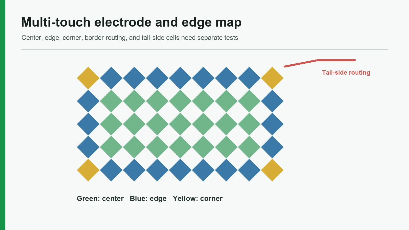
4. Design PCAP Edge Performance as a Separate Region
PCAP edge performance differs from centre performance because the electric field and neighborhood are asymmetric. An interior node is surrounded by adjacent cells; a boundary node has no matching neighbor beyond the active area. Border traces, shields, bezel metal, adhesive termination, display ground, and coordinate clipping also concentrate near the perimeter. Corners combine two boundaries and deserve their own test class.
Infineon AN234185 recommends terminating active-area sides with half diamonds and describes extending the sensing pattern 0.3–0.5 mm beyond the viewing area as a starting approach for edge response in its architecture. These values are not a universal bezel recipe. Mechanical tolerance, cover printing, controller linearization, enclosure overlap, edge gesture behavior, and the selected conductor process still determine the released geometry.
Separate four concepts in the drawing:
- Viewing area: the display region intended to be visible.
- Touch active area: the coordinate region in which contacts are expected to report.
- Edge test area: a defined band of width W used to group boundary results.
- Physical sensor extent: the actual electrode pattern, which may extend past the viewing or reported coordinate boundary.
IEC 62908-12-10:2025 provides a useful measurement vocabulary. Its direct-accuracy method separates centre and edge areas, uses a declared edge width W, and reports maximum, mean, and standard deviation for each region. It does not impose one universal tolerance. The OEM must set the probe, grid, repetitions, edge width, and pass limits.
Microsoft’s touch-display requirements offer one objective reference set for the stated Windows context: ±1 mm outside the edge region, ±2 mm within 3.5 mm of an edge, and stationary jitter no greater than 0.5 mm. Those values are helpful when a project lacks vocabulary, but an industrial HMI, medical interface, automotive display, or marine controller may need different tolerances and failure behavior.
| Region | Geometry review | Coordinate review | Disturbance review |
|---|---|---|---|
| Centre | Repeated full cells and uniform pitch | Mean error, maximum error, linearity, jitter | Display, charger/power, RF and glove states |
| Straight edge | Half/partial cells, pattern extension, border routes | Inward/outward bias, clipping, edge gesture start | Bezel coupling, edge grip, moisture path |
| Corner | Two-axis termination and nearby route fan-out | Radial bias, corner reach, diagonal tracking | Chassis fastener, gasket, shield and tail proximity |
| Tail-side edge | Hot-bond, dense routing and controller proximity | Local distortion and channel imbalance | Flex movement, connector, host-board noise |
the specification states whether a finger centre may cross the visual boundary, how the controller clips coordinates, and what error is acceptable in centre, straight-edge, corner, and tail-side zones.
a supplier is asked for “zero bezel” while traces, cover printing tolerance, enclosure overlap, and edge acceptance remain undefined.
5. Treat Capacitive Sensor Routing, Border, and Tail as One Network
Capacitive sensor routing is part of the sensing network. A long Rx run, an extended Tx/Rx parallel section, a crossover, a dense hot-bond fan-out, or a flex above chassis metal can change channel loading and noise pickup. The border drawing therefore needs electrical review, not only a mechanical width check.
Renesas’ CTSU Electrode Design Guide tells designers to separate Tx and Rx, avoid close parallel routing, cross on different layers near 90° when necessary, and minimize route length and vias. Texas Instruments reaches the same directional conclusion in its TIDUBK4 Noise-Tolerant Capacitive-Touch HMI Design Guide. Routes sense, too. Renesas’ published 20 pF parasitic and 560 Ω–1 kΩ circuit-resistance guidance belongs to the documented CTSU context; it is not a generic acceptance limit for every transparent PCAP matrix. TI and Microchip give the same directional lesson—control Tx/Rx coupling and keep sensitive receive routes short—while their numerical details differ by architecture.
Choose border topology with the channel RC budget
| Topology | When it may fit | What it buys | Main cost or risk |
|---|---|---|---|
| Single-side routing | Small or moderate panels with adequate border and acceptable resistance | Simpler hot-bond and tail | Long routes on the far side; channel imbalance |
| Double routing | Larger or high-aspect-ratio matrices where one-axis resistance is excessive | Shorter effective electrode path and lower RC delay | More contacts, fan-out area and assembly complexity |
| Split-side routing | Packaging permits tails or bonds on more than one side | Short border paths and distributed channel escape | Multiple interconnect zones, service complexity and synchronization constraints |
| Active tail | Controller can sit on the flex close to the sensor | Shorter analog sensor paths | Flex electronics, heat, ESD, bend and replacement concerns |
| Passive tail | Controller belongs on a host PCB | Simpler sensor tail and service separation | Longer analog routes and stronger dependence on host-board layout |
Single, double, and split routing solve different resistance and border constraints. Double routing can reduce row/column RC delay in the architecture documented by Infineon AN234185. An active tail places the controller near the sensor; a passive tail carries sensor lines to a remote host board. Neither topology is automatically superior. Border width, tail length, controller package, channel resistance, display/chassis coupling, ESD path, connector count, flex motion, assembly sequence, repair policy, and thermal environment all belong in the choice.
The routing drawing should label Tx, Rx, shield/guard, chassis or ESD ground, unused conductors, test features, and all layer transitions. Specify where crossovers occur and how their coupling is controlled. At the hot-bond or connector, record pad pitch, alignment datum, contact metallurgy, stiffener, insertion orientation, bend keep-out, and mating cycles only when supported by the selected connector/flex data.
Use the controller vendor’s parasitic-capacitance and resistance model—not an article’s generic number—to review each channel. Look at distribution as well as maximum. A panel whose average channel passes can still show a tail-side baseline gradient if route length and overlap differ sharply across the matrix.
the design review includes a per-channel or per-group resistance/loading estimate, an annotated crossover plan, and a reason for the selected active/passive tail boundary.
the mechanical drawing shows a narrow black border but omits the electrode-to-hot-bond routes that must fit beneath it.
6. Freeze Cover, Adhesive, Display, and Controller Together
The cover lens is a dielectric in the touch signal path. Its material, thickness, coatings, adhesive, decorative ink, local air gaps, curvature, and distance from the finger change coupling. The display and chassis sit on the other side of the sensor and change baseline capacitance and noise. A statement such as “supports 6 mm glass” is incomplete without the controller generation, electrode geometry, glass type, adhesive, display gap, ground structure, finger or glove, and SNR criterion.
A thicker cover reduces touch capacitance and may require larger or more interdigitated electrodes. Overlay performance also depends on geometry, adhesive, SNR, ESD, and controller generation. Context controls the number. These design relationships do not establish a transferable finished-product maximum.
Freeze the following stack fields by drawing revision:
| Stack field | Why it changes the result | Approval evidence |
|---|---|---|
| Cover material and thickness map | Dielectric constant, thickness and local curvature affect coupling | Supplier drawing and measured thickness locations |
| Coatings and decorative ink | Conductive or high-loading layers can distort local fields | Material identity and keep-out review |
| Bonding adhesive | Thickness variation or voids change sensor-to-cover spacing | Bond specification and void/registration criteria |
| Sensor-to-display gap or bond | Display proximity changes loading and noise coupling | Cross-section with tolerance and display model |
| Chassis, gasket and fasteners | Grounded/floating metal near edges changes boundary fields | Enclosure drawing and ground-state definition |
| Controller and firmware | Scan frequency, gain, filters, interpolation and rejection are controller-specific | IC part number plus configuration/firmware revision |
Assign one integration owner. The sensor fabricator can inspect artwork and resistance; the controller vendor can interpret channel limits; the display integrator can characterize display noise; the mechanical team controls the cover, bond, gasket, and chassis; firmware owns tuning and coordinate behavior. Microchip’s companion AN4162 maXTouch PCB Layout Guidelines illustrates why sensor and controller-board layout cannot be separated. Someone must close the loop and maintain a compatible revision set.
The controller should be selected early enough to influence pattern and routing. Late substitution can change channel mapping, allowed load, shield strategy, scan timing, firmware tools, host protocol, EMC behavior, and available edge algorithms. A “pin-compatible” controller change is not automatically sensor-compatible.
7. Run a Five-Step Design and Sourcing Process
The following process turns the engineering framework into a quotable, testable package. It also keeps published application-note values in their proper role: starting evidence rather than copied specifications.
Step 1 — Freeze use conditions and coordinate boundaries
Issue one requirement sheet covering active/viewing dimensions, orientation, required gestures, concurrent contacts, contact object, glove or stylus, minimum separation, edge-zone behavior, invalid-input policy, report/latency requirement, and host interface. Add dry, wet, cleaning, temperature, display, power, and enclosure conditions relevant to the product.
Step 2 — Build the channel–pitch–stack worksheet
Compare at least two feasible pitch/matrix options against the selected controller’s channel count, RC/loading guidance, scan constraints, and firmware feature set. Record the complete cover–adhesive–sensor–display–chassis cross-section. Treat published Infineon or Microchip dimensions as attributed candidates, not released requirements.
Step 3 — Review electrode, edge, border, and tail in one drawing
Show interior, straight-edge, corner, and tail-side cells; active and viewing boundaries; Tx/Rx map; all border routes; crossovers; shield/ESD structures; hot-bond; tail stack; connector; datums; and keep-outs. Require evidence that the chosen conductor process can hold critical gaps, registration, resistance, and optical appearance.
Step 4 — Prototype the production-intent stack
Use prototyping to test the intended cover, adhesive, display model, chassis, cable, connector, controller, and firmware branch—not a loose sensor on an evaluation board alone. Log every substitution. A prototype with thinner glass or a quieter display answers a different question.
Step 5 — Approve against the centre–edge–corner matrix
Freeze the test script before samples arrive. Identify probe/finger/glove, points, trajectories, contact combinations, repeats, edge width, pass rate, error calculation, jitter definition, invalid-contact behavior, recovery time, and electrical/environmental states. Approval attaches to the complete revision set, not the sensor drawing by itself.
8. Release Blockers and Cases Where the Recommended Construction Is Wrong
The framework recommends a co-designed mutual-capacitance matrix with controlled edge cells and routing. That construction is not always the best choice.
- Input cannot couple reliably through the required interface. A nonconductive passive stylus, very thick insulating glove, or unusual interaction surface may favor another input technology unless a validated controller/stylus solution exists.
- The interface must work during uncontrolled liquid films. PCAP can support designed wet modes, but it should not be chosen on the promise that every droplet, stream, pooled film, cleaner, or gloved wet hand will behave correctly.
- The active surface is strongly curved or has variable cover thickness. A standard planar diamond matrix may produce uneven fields; controller-supported custom geometry or a different sensing architecture may be needed.
- The border is narrower than the route and tolerance budget. Active-area routing or specialized edge structures can reduce borders, but they add coupling, optical, process, patent, and tuning risk. A slightly wider border may be the lower-risk system choice.
- The controller must be chosen after the sensor is tooled. If channel limits, loading, scan timing, and tuning cannot be frozen, a custom pattern release is premature.
- The product requires simple discrete commands, not coordinates or gestures. A membrane switch, sealed mechanical control, or a small set of capacitive buttons may provide clearer feedback and a simpler validation burden for some industrial control interfaces.
- A standard off-the-shelf module meets the envelope. Custom electrode artwork adds engineering, tooling, validation, and change-control work. Do not customize merely to use the full enclosure window.
Disqualify a proposal if it offers an edge-accuracy or cover-thickness guarantee without identifying the stack and controller, omits border routes, treats firmware as an unspecified supplier default, or replaces installed-system validation with a centre-point finger demonstration.
9. Validate Centre, Edge, and Corner on the Final Assembly
A production-intent test matrix must expose geometry, routing, stack, controller, and enclosure interactions. Test the corners. Testing and validation should cover the assembled HMI because a loose sensor cannot reproduce display emissions, chassis coupling, final grounding, cover tolerances, cable routing, or enclosure edge effects.
| Test block | Centre | Straight edge | Corner / tail side | Record |
|---|---|---|---|---|
| Static accuracy | Grid points and repeated touches | Points inside declared edge width W | Corner targets and hot-bond-side points | Mean, maximum, standard deviation, pass rate |
| Moving linearity | Horizontal, vertical, diagonal paths | Paths entering and tracking along edges | Diagonal corner entry and exit | Path error, dropped reports, clipping |
| Stationary jitter | Light/nominal/heavy contact if relevant | Edge targets near bezel | Tail-side and grounded-fastener proximity | Peak-to-peak or declared statistic and duration |
| Multi-contact separation | Required two- and multi-finger layouts | One contact centre, one near edge | Contacts near adjacent edges/corner | Resolved contacts, swaps, merges, ghosts |
| Gesture behavior | Pinch, rotate, swipe, project-specific commands | Gesture start/end at boundary | Corner-origin gesture where required | Recognition, latency, false activation |
| Contact-object states | Bare finger, defined glove/stylus | Same objects at edges | Worst posture and tail-side area | Detection and coordinate error |
| Display/power disturbance | Intended images, brightness, refresh and power states | Repeat worst centre condition | Repeat near routes and connector | Noise, false touches, recovery |
| Moisture/cleaning | Defined droplets, wet finger, film or wipe | Edge and gasket paths | Corner accumulation paths | Valid/invalid reports and recovery state |
| EMC pre-compliance | Project-selected ESD/RF setup | Accessible cover and bezel locations | Connector, seam and chassis locations | Configuration, level, criterion, anomalies |
IEC 62908-12-10:2025 supports separate centre and edge statistics, but the OEM must supply acceptance values. Microsoft’s Physical Input Position and Edge Test is one useful example: it includes edge-entry scenarios and a 95% pass rate in its platform context. Do not silently adopt the Microsoft probe, tolerance, or pass rate for another product.
Electrical disturbance belongs in the same validation revision. IEC 61000-4-2:2025 defines ESD immunity methods, while IEC 61000-4-3:2020 defines radiated-RF immunity methods. They are basic EMC standards, not proof that a loose panel is compliant. The applicable product standard and system owner select levels, coupling locations, performance criteria, recovery behavior, and test configuration. The related touch-panel EMI and ESD design guide should be used to prepare the electrical integration review.
Before approval, compare channel baselines and signal metrics across the matrix where the controller exposes them. Look for gradients near long routes, the tail, chassis features, and display drivers. Archive raw data, controller logs, firmware/configuration, display part and settings, mechanical revision, environmental state, and sample serial numbers. A screenshot labeled “PASS” is not enough for change control.
10. Project Input and Sample-Approval Checklist
Send a coherent package rather than separate mechanical and electrical fragments.
Drawing and controller inputs
- cover outline, viewing area, touch active area, enclosure opening, origin, orientation, and dimensional datums;
- display model, active-pixel area, frame/ground construction, intended brightness/refresh states, and sensor-to-display spacing;
- cover material, nominal and local thickness, coatings, decorative ink, adhesive, bond tolerance, and permitted voids;
- required gestures, simultaneous contacts, contact objects, minimum separation, edge behavior, latency/reporting and host interface;
- candidate controller, channel map, firmware/configuration owner, communication interface, supply and grounding concept;
- tail exit, length envelope, bend zones, connector and mating orientation, controller-on-flex decision, and service boundary;
- applicable ESD/RF/product standards plus project-selected levels and functional criteria;
- conductor process, optical limits, critical pattern features, resistance targets, registration datums, inspection and traceability.
Sample approval inputs
- production-intent cover, sensor, adhesive, display, chassis, cable, connector, controller and firmware revisions;
- centre/edge/corner point map and declared edge width W;
- finger/probe, gloves, stylus, moisture, cleaning and invalid-contact set;
- static, moving, jitter, separation, gesture, recovery and false-touch acceptance criteria;
- display patterns, power/charger states, grounding variants and environmental conditions;
- sample count, repeat count, pass-rate rule, raw-data format, anomaly handling and change/retest trigger.
11. Send the Active Area and Gesture Requirements
To begin a defensible review, send the active area and gesture requirements together with the cover/display cross-section, candidate controller, edge requirement, tail direction, and enclosure opening. JASPER can then be considered as one PCAP panel option within the project’s controller and validation boundary.
The useful first response is not a generic pitch or bezel promise. It is a list of closed assumptions, conflicts, missing evidence, controller-dependent items, and the prototype tests needed before release. Keep the sensor artwork, firmware configuration, stack drawing, and acceptance matrix under one revision set.
12. Frequently Asked Questions
What electrode pitch should a capacitive multi-touch panel use?
There is no universal pitch. Infineon AN234185 documents 3.8–5.0 mm, with 5 mm typical, for its interleaved-diamond context; Microchip AN2934 gives 4–10 mm, with 6 mm typical, for several mutual surfaces. Select pitch against finger size, accuracy, contact separation, channel count, RC load, cover stack, conductor process, and controller guidance.
How are channel count and electrode pitch related?
Smaller pitch across the same active area usually requires more Tx and Rx electrodes. Physical channel demand is approximately `Ntx + Nrx`, while mutual sensing nodes are approximately `Ntx × Nrx`. Confirm both the controller pin/channel limit and its ability to scan the actual resistance and parasitic load at the required rate.
Does a diamond electrode pattern guarantee multi-touch performance?
No. A diamond pattern creates a matrix suitable for mutual-capacitance position sensing, but simultaneous-contact count, separation, accuracy, latency, water/glove behavior, and false-touch rejection also depend on the controller, firmware, SNR, cover/display stack, routing, grounding, and host processing.
What causes poor PCAP edge performance?
Edge cells have asymmetric neighbors, and the perimeter also contains border traces, shields, bezel metal, adhesive boundaries, display ground, and coordinate clipping. Use explicit half/partial edge cells, active/viewing-area boundaries, controlled routing, controller linearization, and separate straight-edge, corner, and tail-side tests.
Should the sensing pattern extend beyond the display viewing area?
It can. Infineon AN234185 describes a 0.3–0.5 mm extension as a starting approach in its architecture. The released value must account for cover printing, mechanical tolerance, enclosure overlap, edge-cell geometry, routing, controller mapping, and the project’s declared edge test region.
How should Tx and Rx traces cross?
Avoid crossings when practical. Renesas, TI, and Infineon guidance favors separating Tx and Rx, avoiding long parallel runs, and crossing on different layers near 90° when a crossing is necessary. Keep the overlap short and use controller-approved shielding or spacing; do not confuse a 90° crossing with a 90° trace bend.
Is an active flex tail better than a passive tail?
Not automatically. An active tail can place the controller close to the sensor and shorten analog routes, but it adds electronics, ESD, heat, bend, assembly, and service constraints on the flex. A passive tail simplifies the sensor but makes host-board routing and connector coupling more critical. Compare both against the full system.
How should an OEM specify PCAP edge accuracy?
Define a centre area and an edge band of width `W`, then specify the probe, grid or paths, repetitions, statistics, tolerance, pass rate, coordinate clipping, and corner treatment. IEC 62908-12-10:2025 supplies a measurement framework; the OEM or applicable product standard supplies the acceptance limits.
When is a custom projected-capacitive matrix not the best choice?
It is a poor choice when a standard module already meets the envelope, when the controller and final stack cannot be frozen, when the required input cannot couple reliably, or when simple discrete controls would be safer and easier to validate. Extreme liquid, curvature, border, glove, or noise requirements may also favor another architecture.
Technical References
- Source: Infineon AN234185 Touch Sensor and Electrode Design. Accessed 2026.
- Source: Microchip AN2934 Mutual Capacitance Touch Surface Design. Accessed 2026.
- Source: Texas Instruments CapTIvate Technology Guide. Accessed 2026.
- Source: Renesas Capacitive Touch Sensor Design Guidance. Accessed 2026.
- Source: Microsoft Touchscreen Device Requirements. Accessed 2026.
- Source: AN234185 touchpad design guide. Accessed 2026.
- Source: QTAN0080 maXTouch Sensor Design Guide. Accessed 2026.
- Source: AN2934 Capacitive Touch Sensor Design Guide. Accessed 2026.
- Source: IAAT818X automotive multitouch controller. Accessed 2026.
- Source: CapTIvate Design Guide. Accessed 2026.
- Source: Journal of Display Technology study. Accessed 2026.
- Source: 62908-12-10:2025. Accessed 2026.
- Source: touch-display requirements. Accessed 2026.
- Source: CTSU Electrode Design Guide. Accessed 2026.
- Source: TIDUBK4 Noise-Tolerant Capacitive-Touch HMI Design Guide. Accessed 2026.
- Source: AN85951 CAPSENSE Design Guide. Accessed 2026.
- Source: AN4162 maXTouch PCB Layout Guidelines. Accessed 2026.
- Source: Physical Input Position and Edge Test. Accessed 2026.
- Source: 61000-4-2:2025. Accessed 2026.
- Source: 61000-4-3:2020. Accessed 2026.
Review the complete capacitive touch stack before release
Send the cover, artwork, active area, display, electrode, controller, tail, environment, and acceptance states for an engineering review.