
A backlit capacitive touch panel succeeds only when the graphic, optical, sensing, and control layers are engineered as one stack. This guide helps HMI, electrical, quality, and sourcing teams decide how to align dead-front ink, illuminated touch icons, LEDs, electrodes, and controller tuning—and how to approve the result under defined viewing and operating conditions.
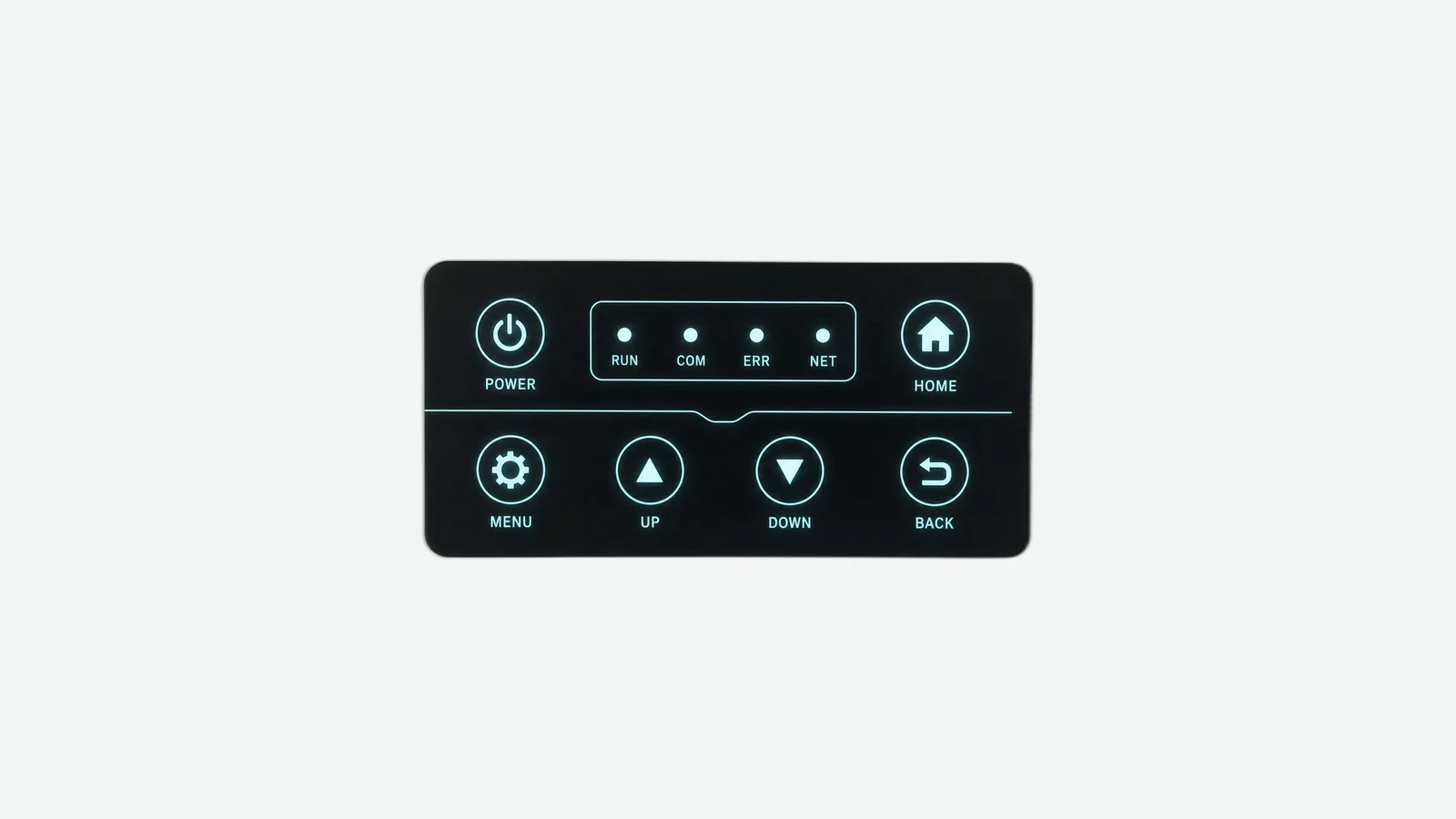
A dark-room photograph cannot approve this interface. The off state must hide inactive graphics under the specified ambient light, while the powered state must reveal the right icon without hot spots, bleed, objectionable color shift, or lost touch margin. No universal ink density, LED pitch, or sensitivity setting satisfies every cover lens. The final decision belongs to measured samples built with the production-intent stack.
What a Dead Front Capacitive Switch Must Control
A dead front capacitive switch is a touch interface whose selected symbols are visually suppressed when their light source is off and revealed when it is on. “Dead front,” “hidden until lit,” and “secret until lit” describe the optical behavior, not the sensing method. The touch electrode may remain active while its icon is dark, or firmware may disable the function at the same time.
Two appearance states must therefore be specified separately:
| Appearance state | Required observation | Controlled conditions |
|---|---|---|
| Off | Icon, window edge, print halo, electrode, adhesive, and internal hardware remain within the released concealment limit | Ambient source, illuminance, observer distance, and viewing angles |
| Lit | The intended symbol is readable without bright points or light leaking into adjacent functions | Drive current, supply voltage, temperature, viewing angle, and ambient light |
Sanwa Screen USA describes true dead-front behavior in the same two parts: graphics should be near-invisible while unlit and evenly revealed without shadows or bleeding when illuminated (Sanwa, 2025). Those words are useful requirements, but they are not acceptance limits. A drawing still needs measurable conditions and a signed appearance sample.
The design decision is not simply “black ink plus LEDs.” It is a balance. More masking improves off-state concealment but removes useful light. A thicker diffuser can smooth an LED image yet move the finger farther from the electrode. Higher LED current raises luminance but also changes thermal conditions, power demand, color, and sometimes capacitive noise. A visually excellent face can still have poor touch signal-to-noise ratio (SNR).
This is why the work belongs upstream, before final artwork, board routing, or firmware tuning is frozen.
The Coordinated Stack of a Backlit Capacitive Touch Panel
A useful stack drawing names the function of every layer and shows which team owns it. JASPER's backlit capacitive panels page covers the related product construction; the section below focuses on the engineering interfaces that must be frozen together.
USER / AMBIENT LIGHT
1. Cover surface
Glass, PMMA, polycarbonate, coating, texture, gloss
2. Graphic and dead-front ink stack
Background color, icon aperture, neutral-density/mask layers,
color-correction ink, registration datums
3. Optical coupling layer
Clear adhesive, diffuser, light-guide film, spacer or cavity
4. Capacitive sensor layer
Copper, silver, ITO/PEDOT or another validated conductor;
button electrode, traces, guard/shield and keep-outs
5. Light source and isolation features
Top-fire/side-fire LED, reflector, separator walls, masks,
extraction pattern, PCB and thermal path
6. Bonding and enclosure interface
Adhesive gasket, datum scheme, bezel/chassis and seal path
7. Controller and firmware
Baseline tracking, thresholds, filtering, debounce,
moisture strategy, LED drive/PWM and diagnostics
Texas Instruments models the basic coupling as C = εr ε0 A/d: dielectric constant (εr), electrode area (A), and distance (d) affect capacitance. Its CapTIvate design guide lists representative dielectric constants of 1.0 for air, 2.8 for acrylic, 2.9–3.0 for polycarbonate, and 7.6–8.0 for glass. Actual values depend on material formulation, but the direction is clear: changing the cover or introducing an air gap changes the sensor, even when the artwork and PCB do not move (Texas Instruments, CapTIvate Design Guide).
Infineon's AN85951 makes the same system point. Finger capacitance falls as overlay thickness rises; conductive paint can disturb the electric field; and intimate contact with a nonconductive adhesive helps by removing air gaps. For smooth glass or acrylic, Infineon gives approximately 60 µm adhesive as an example, while roughly 130 µm can accommodate minor irregularities. These are controller-vendor examples, not universal bond-line specifications (Infineon, AN85951).
The optical layers and sensing layers cannot be released independently. An icon window that forces a cutout through the electrode may lower sensitivity. A transparent electrode may solve that obstruction but introduce visible patterning, sheet-resistance constraints, or another print pass. A cavity that fixes a hot spot may add a low-dielectric gap. Each correction moves another variable.
The Nine-Point Evaluation Framework
The following nine criteria convert appearance language into buildable requirements. They run in dependency order: visual states first, then materials and geometry, then light, sensing, sample approval, and system validation.
1. Define the Off State and Lit State Before Selecting Ink
The visual specification should begin with two scenes, not a color chip. For the off state, document illuminance at the panel, illuminant or ambient source, observer distance, viewing-angle range, background adaptation, and whether faint icon read-through is acceptable. For the lit state, add LED current or PWM duty, stabilization time, supply tolerance, icon state, and minimum/maximum operating temperature.
A ratio or measured difference is more transferable than “invisible.” The numerator and denominator still need defined measurement locations. Comparing an icon center with adjacent background at normal incidence will not reveal a halo seen at 45 degrees, so the drawing and golden sample should govern together.
The appearance specification contains separate off-state and lit-state photographs or renderings, measurement geometry, ambient condition, and signed physical samples.
The requirement says only “piano black when off” or “bright, even icons,” and the supplier is expected to infer the viewing environment.
2. Freeze the Cover, Surface Finish, and Ink Stack Together
Cover-lens color is part of the filter. Clear glass with a black rear print behaves differently from smoke-tinted glass, hard-coated polycarbonate, or textured PMMA. Surface gloss changes reflections in the off state. A matte texture may hide internal detail but scatter the lit symbol. Ink chemistry, layer count, mesh, cure, print side, and substrate pretreatment affect both transmitted light and appearance.
For designs using glass, glass nameplates need the same attention to decoration side, edge treatment, surface finish, and bonding as the touch sensor. For film constructions, the graphic overlay construction must also account for forming, hard coat, print registration, and adhesive compatibility.
A useful optical coupon includes the actual cover material and finish, several candidate ink builds, the intended icon colors, and both large and narrow graphic features. It is measured over the selected light source, not approved on a white inspection table alone.
The bill of materials identifies substrate grade, thickness, tint, finish, ink system, print sequence, cure window, and approved transmission or appearance coupon.
Artwork receives final approval while ink is still described as “opaque black,” without a current technical datasheet or lit coupon.
3. Put Icon and Electrode Geometry on One Datum System
An illuminated icon and its touch electrode have different jobs, but users expect them to coincide. The artwork origin, sensor origin, PCB origin, housing datums, and inspection datums should resolve into one coordinate system. The tolerance stack must include printing, laser or die cutting, adhesive lamination, FPC/PCB registration, LED placement, enclosure location, and cover placement.
The electrode need not copy the icon outline. A ring or segmented conductor may leave an optical path through the center; a solid electrode may work beside or behind a diffuser; a transparent conductor may cross the light path. Texas Instruments and Infineon both treat electrode size, spacing, traces, ground and surrounding conductors as sensing variables, so an optical cutout cannot be added late without rechecking performance (TI; Infineon).
Eastprint documents one projected-capacitive build with 16 screen-print passes, transparent PEDOT, silver, carbon, dielectric layers, a diffuser, and registration control. That is a useful proof of interaction—not a default recipe for every panel (Eastprint project data).
The released package has common datums, nominal icon/electrode centers, keep-outs, registration tolerances, and an analysis of the worst combined offset.
Optical artwork and circuit data use different origins, or a supplier receives only a rendering and a separate Gerber file.
4. Select the Lighting Architecture From Geometry, Not Habit
Direct LEDs, edge-lit light guides, diffuser cavities, and transparent or annular electrodes solve different constraints. Icon area, pitch, cover thickness, available depth, power, heat, color count, animation, and neighboring dark zones should drive the choice.
A thin light guide reduces interruption of the capacitive field, while side-firing LEDs and a designed extraction pattern improve uniformity in the documented GLT construction. A light guide is not automatically uniform. Its extraction pattern, edge coupling, reflector, distance from the icon, cutouts, compression, and assembly tolerances still matter.
Direct top-fire LEDs can be efficient for small, isolated symbols but expose the die image if spacing and diffusion are inadequate. A common light guide can serve many icons but may cross-feed light. A cavity with physical separators can isolate functions yet consume depth. Transparent conductors open the optical aperture but introduce their own visual and electrical tradeoffs.
The supplier explains why the selected architecture fits icon size, spacing, package depth, power and touch margin, supported by a coupon or optical model.
LED quantity and pitch are copied from a previous panel with a different cover, icon geometry, ink transmission, or viewing condition.
5. Specify the LED by Part, Bin, Current, and Thermal Condition
“White LED” is not a procurement specification. Release the source and drive conditions as controlled BOM and drawing fields.
| LED control field | Minimum released definition | Why it matters |
|---|---|---|
| Source | Manufacturer, orderable part, package, and approved substitutions | Package optics and electrical limits change the lit face |
| Color and output | Chromaticity or color bin plus intensity or flux bin | Nominal CCT or a screen color cannot control lot variation |
| Electrical drive | Forward-voltage range, current, PWM frequency, and duty range | Output, temperature, EMI, and touch noise depend on the operating point |
| RGB control | Per-channel current limits, mixing method, calibration, and transition behavior | Color balance changes across state and temperature |
| Lot policy | Bin mixing rule, traceability, and substitution approval | Uncontrolled mixing creates visible panel-to-panel differences |
Vishay's LED portfolio separates package formats, colors, low-current/standard/power families, and backlighting applications; listed SMD formats range from 0402 and 0603 to MiniLED and PLCC packages (Vishay LED portfolio). That breadth shows why package name or nominal color alone is insufficient. The selected part's current datasheet and bin tables are the controlling sources.
Temperature changes forward voltage, output, and perceived color. PWM can preserve one operating point better than deep analog current variation in some designs, but it may introduce EMI, camera banding, audible interaction, or touch-scan timing issues. The controller and LED driver should therefore be reviewed together.
The drawing and BOM control orderable parts, acceptable bins, current conditions, substitutions, thermal assumptions, and lot-mixing policy.
The requirement lists only CCT, a hex color, or “high-brightness LED,” with no bin or operating condition.
6. Tune Touch on the Final Optical and Mechanical Stack
Capacitive tuning performed on a bare PCB is an experiment, not final validation. The released stack adds cover material, inks, adhesive, diffuser or cavity, electrode construction, LED routing, chassis metal, bezel, gasket, cable, ground, power noise, moisture, gloves, and manufacturing variation.
Texas Instruments recommends measuring SNR and design margin after first-pass tuning. Infineon treats parasitic capacitance from electrodes, traces, vias, grounds and chassis conductors as part of the sensor baseline. Both sources support the same rule: tune and stress the production-intent assembly, not an electrically convenient surrogate.
LED PWM deserves a specific check. Run touch scans with all icons off, each icon on, all channels on, minimum and maximum duty, supply corners, and any animation pattern. Then repeat at temperature and with the intended overlay condition. If the controller supports scan synchronization, spread-spectrum clocks, driven shields, baseline tracking, or liquid-tolerance modes, document the configuration rather than assuming defaults.
The approval report contains raw/baseline counts, touch delta, noise, SNR or the controller vendor's equivalent margin, thresholds, debounce, scan timing, and worst-case test states.
A demonstration video proves finger response at room temperature, but no margin data or final-stack configuration is retained.
7. Control Hot Spots, Bleed, and Optical Cross-Talk at Their Source
A bright point is usually an optical path problem, not an instruction to add another print layer everywhere. Diagnose the path: LED die image, insufficient source-to-icon distance, thin diffusion, low mask density, reflector discontinuity, extraction-pattern error, cavity leak, adhesive edge, or registration shift. Each cause calls for a different correction.
Masks should block light where it is unwanted without becoming visible in the off state. Separator walls need enough optical density and mechanical stability. Diffusers should be evaluated for both uniformity and transmission. An edge-lit guide needs extraction features scaled to distance from the LED; a uniform dot pattern rarely produces uniform output across an irregular panel.
Evaluate neighboring states, not just one symbol. A warning icon beside a frequently lit status symbol may ghost even when each looks acceptable alone. Photographing with automatic exposure can hide this problem, so approval must rely on fixed exposure plus instrument readings.
The test pattern cycles one icon, adjacent pairs, all icons, maximum-current white, RGB primaries if present, and off-state recovery after lighting.
Only one face-on photograph in a dark room is supplied, with no fixed exposure, measurement map, or adjacent-icon state.
8. Make the Golden Sample a Measured Object
A golden sample is useful only when it points back to data. Identify its build revision, material lots, ink passes, LED lots/bins, controller firmware, settings, assembly date, and measurement report. Seal and store it so later comparisons do not rely on an aging, scratched, or undocumented part.
For color, ISO/CIE 11664-6:2022 defines the CIEDE2000 formula for differences based on CIELAB values under stated reference conditions. The standard excludes areas perceived as primary emitting light sources from its stated scope. A backlit icon should therefore retain measured luminance and chromaticity data, while ΔE00 may be used only where the measurement setup and scope are appropriate (CIE / ISO).
For brightness, record a point map or image-based luminance map and calculate the declared statistic—such as minimum/average—using a fixed region of interest. For the off state, record icon and background readings under the agreed ambient source and angles. Never compare supplier photographs taken with different camera exposure.
The signed sample, raw data, calculation method, instrument, geometry, stabilization time, ambient condition and firmware revision are traceable.
“Match approved sample” appears on the drawing, but the sample has no serial number, measurement report or configuration record.
9. Validate the Finished Assembly Against Product Requirements
Component screening and finished-equipment validation answer different questions. IEC 61000-4-2:2025 defines a common, reproducible method for evaluating equipment immunity to electrostatic discharge, including test equipment, setup, procedure, calibration and test-level ranges. The IEC explicitly leaves the applicable tests and severity to product committees or product requirements (IEC 61000-4-2:2025).
IEC 60529 classifies protection provided by enclosures against access, solid objects and water (IEC 60529). A touch-panel component or adhesive gasket does not establish the finished enclosure's IP code. Bezel geometry, fasteners, cable exits, housing stiffness, gasket compression, aging and assembly process all contribute.
Validation should also cover supply variation, temperature, humidity/condensation where applicable, cleaning agents, UV exposure where applicable, glove use, water films, conducted/radiated noise, adjacent metal, and mechanical stress from assembly. The applicable levels come from the product's environment and regulatory plan—not from a generic blog table.
Component and assembly testing is linked to a product-level validation matrix with defined modes, severity, functional criteria and post-test inspection.
A material datasheet, controller reference board, or component test is presented as proof that the complete device meets an IP or EMC requirement.
Choose a Capacitive Panel Backlighting Architecture
The best architecture is the one that meets optical and sensing limits with controllable production variation. The table is a screening tool; prototype coupons must settle the choice.
| Architecture | Best fit | Main advantage | Main design risk | Evidence to request |
|---|---|---|---|---|
| Direct top-fire LED behind each icon | Small, isolated icons with enough stack depth | Simple channel control and efficient local lighting | Die image, hot spot, shadow from electrode or hardware | Source-distance coupon, luminance map, adjacent-icon bleed test |
| Edge-lit light-guide film | Many icons across a thin, broad panel | Shares a small number of side-firing LEDs and can smooth large areas | Extraction pattern, edge coupling and cross-feed vary with geometry | Production-intent guide, extraction artwork, compression test, full-state map |
| Diffuser cavity with separators | Functions requiring strong optical isolation | Physical walls can suppress bleed between nearby icons | More depth, parts, assembly tolerances and cavity reflections | Sectioned prototype, wall/mask density, tolerance analysis, thermal check |
| Transparent or annular electrode path | Icon must occupy the electrode center | Preserves an optical aperture through the sensing zone | Sheet resistance, conductor visibility, pattern registration, changed touch margin | Conductor sample, resistance map, haze/visibility check, final-stack SNR |
Epec describes annular electrodes, transparent conductors, and lighting above the circuit as three integration routes (Epec, 2020). None is inherently superior. A ring electrode can suit one button yet perform poorly beneath a thick cover; transparent ink can pass light but remain visible under some angles; a light source above the sensor can complicate routing and lamination.
When dead-front construction is not the best choice
Do not use hidden-until-lit graphics as the only communication method when a safety label, emergency function, hazard warning, or critical control must remain identifiable with power removed. An always-visible printed legend, mechanical control, separate indicator, or redundant labeling may be required by the product risk assessment.
Dead front may also be a poor choice for a low-power product that cannot afford the necessary illumination, a sunlight-readable interface where inactive controls must remain obvious, a shallow package with no workable optical path, or a low-volume program that cannot support iterative ink coupons and optical approval. A conventional printed overlay can be the more honest engineering decision.

How to Approve a Backlit Capacitive Touch Panel
The process below prevents the usual handoff failure in which industrial design approves the face, electrical engineering approves a bare sensor, and sourcing asks a supplier to reconcile both after tooling.
Step 1 — Issue one coordinated input package
Send vector icon artwork; nominal icon and electrode centers; cover dimensions, material, thickness, tint and finish; intended viewing angles; ambient-light scenes; available depth; enclosure data; LED voltage/current budget; controller choice; interface; operating environment; cleaning chemicals; glove and moisture expectations; and regulatory test inputs. The custom capacitive touch panel design inputs should share revision control with the mechanical and electrical drawings.
Drawing checklist
| Discipline | Minimum release input |
|---|---|
| Optical | Off/lit states, icon colors, ambient scenes, viewing angles, uniformity method, bleed boundary |
| Mechanical | Cover material/finish, total stack, datums, tolerances, keep-outs, bezel, bond/seal geometry |
| Electrical | Electrode/traces, LED part and bin, driver/current/PWM, supply limits, grounding and connector |
| Firmware | Controller, scan mode, thresholds, filtering, baseline, debounce, moisture/glove states, diagnostics |
| Environmental | Temperature, humidity/condensation, UV, cleaners, ESD/EMC inputs, expected contamination |
Step 2 — Build optical coupons before a full functional prototype
A coupon should answer the cheapest high-risk questions: Which ink stack hides the symbol? Which candidate passes enough light? Does the selected cover tint shift icon color? How much source distance or diffusion is needed? Include narrow strokes, broad fills, adjacent colors, a border, and the smallest production icon. Use actual substrate, finish, ink, cure and candidate LEDs.
Do not call a white-table inspection an off-state test. Place coupons in the real ambient scenes, then illuminate them at controlled current. Record instrument data and fixed-exposure images.
Step 3 — Build an electrically active stack
The next sample combines the cover, adhesive, graphics, optical layers, electrode, LED board, enclosure metal and target controller. Measure touch baselines and signal while cycling every lighting state. Include mechanical compression and the actual cable route; both can alter the field or introduce noise.
At this stage, compare architecture alternatives rather than polishing one weak concept. A second diffuser, different LED package, ring electrode, mask change or extra cavity depth may produce a cleaner tradeoff than firmware compensation.
Step 4 — Tune after the stack is dimensionally stable
Controller thresholds should not hide a mechanical or optical defect. First eliminate uncontrolled air gaps, routing violations, floating conductors and LED-driver noise. Then tune baseline tracking, sensitivity, filters, debounce, scan rate, shielding and moisture behavior on representative assemblies.
Touch-margin screen: Use 10:1 worst-condition touch SNR as the first measured acceptance point when the selected controller method supports that calculation. Infineon documents 10:1 in defined CAPSENSE conditions; Texas Instruments requires measured SNR and design margin. Release the final threshold from controller-specific data on the production optical, electrical, and mechanical stack.
Step 5 — Approve a measured golden sample
Freeze the optical map, touch data, material lots, firmware and drawing revision. Sign the sample only after reviewing off-state concealment, lit-state uniformity, color, bleed, viewing angle and all touch states. Define how production samples will be compared and what happens when instruments and visual reviewers disagree.
The golden sample should be accompanied by raw readings and annotated measurement locations. Without those records, it becomes a subjective color reference that cannot diagnose drift.
Step 6 — Validate and lock change control
Run the product-specific optical, touch, environmental, ESD/EMC, cleaning and enclosure tests. Record functional acceptance during and after exposure. Then place ink, substrate, LED, diffuser/light guide, adhesive, electrode process, controller settings and firmware under change control. An “equivalent” LED or black ink is not equivalent until the same tests prove it.
Failure Chain: From Visible Symptom to Corrective Direction
Treat a defect as evidence about the stack. Changing LED current first may hide the cause and create another failure.
| Symptom | Likely interaction | Diagnostic check | Corrective direction to evaluate |
|---|---|---|---|
| Icon visible while off | Ink transmission, surface reflection, window edge, internal contrast | Measure icon/background under specified ambient light and angles | Rebalance mask/neutral-density layers, finish, tint or internal masking |
| Bright center or LED image | Source too close, weak diffusion, clear path through electrode | Luminance map and sectioned stack review | Increase optical mixing distance, redesign diffuser/extraction, alter source package/position |
| Dim but uniform icon | Excess ink/mask loss, low coupling, current limit | Measure transmission coupon and LED operating point | Change ink stack or coupling before raising current |
| Light leaks into adjacent icon | Shared guide/cavity, mask gap, wall reflection, registration shift | Illuminate one channel at a time and inspect tolerance extremes | Add optical isolation, extend masks, revise guide extraction or datum control |
| Like icons show different color | Mixed LED bins, current/temperature variation, ink thickness variation | Record chromaticity, current and temperature by location/lot | Tighten bin/lot rules, thermal path, drive control or print process |
| Touch weak only over lit windows | Electrode aperture, extra optical thickness, air gap, transparent-conductor resistance | Compare raw touch delta/SNR by icon with LEDs off/on | Resize/reposition electrode, remove gap, change conductor, retune final stack |
| False touch when LEDs dim | PWM edge coupling, ground return, supply ripple, scan timing | Correlate raw counts with PWM phase and channel state | Reroute returns, filter/decouple, synchronize scans, revise driver edge rate |
| Works dry, fails with film or gloves | Field geometry, threshold, baseline/liquid mode, cover stack | Repeat vendor-prescribed wet/glove matrix with raw data | Revisit sensor/shield design and validated controller mode; do not only lower threshold |
Sample Approval Test Matrix
Use the matrix to write project-specific limits. The 10:1 SNR screen is one controller-scoped starting point; optical coupons and engineering samples must establish the released luminance, uniformity, color, bleed, registration, touch-margin, and environmental limits.
| Test | Controlled conditions | Record | Approval boundary |
|---|---|---|---|
| Off-state concealment | Defined ambient illuminance/source, normal plus agreed oblique angles, LEDs off | Icon and adjacent-background readings; fixed-exposure images | Project drawing plus signed sample; no hidden auto-exposure |
| Lit luminance and uniformity | Defined current/PWM, supply, stabilization time, ambient, temperature | Point/image luminance map; declared min/average or other statistic | Project-specific measured limit by icon class |
| Color consistency | Selected LED bin/lot, stabilized temperature/current, documented instrument geometry | Chromaticity, CCT where relevant, and applicable color-difference result | Project-specific limit; apply ISO/CIE method only within its stated scope |
| Adjacent-function bleed | One channel, adjacent pairs, all channels, RGB primaries where used | Dark-zone readings and fixed images | No unintended function becomes interpretable at the specified scene |
| Touch margin | Final stack; LEDs off/on/PWM; supply and temperature limits; dry/glove/moisture modes as applicable | Raw/baseline, touch delta, noise, SNR/vendor margin, thresholds | Controller-specific limit; initial screen is 10:1 worst-condition SNR |
| Registration | Production datums and tolerance samples | Icon, electrode, LED and mask offsets | Released geometric tolerance and no optical/touch failure at extremes |
| ESD immunity | Finished assembly, specified operating modes and product test plan | Setup, test points, levels, discharges, functional class, post-test status | Product requirement using IEC 61000-4-2:2025 where applicable |
| Enclosure ingress | Finished enclosure, cable exits and production seal process | Method, exposure, internal inspection, function | Required IEC 60529 classification only after complete-enclosure test |
| Environmental conditioning | Product-defined cold, heat, humidity/condensation, UV and cleaner exposure | Before/after optics, adhesion, touch data and visual condition | Product-specific limits and no prohibited material change |
A verified optical sample is not a beauty photograph. It is an assembly with traceable materials, an instrument map, known electrical conditions, and a record of what passed. Production control should then sample the variables that can recreate the failure: ink deposition, registration, LED/bin/drive, optical spacing, adhesive thickness, touch margin, and final appearance.
Project Inputs and the Concrete Next Step
Before requesting a prototype, assemble four files: the vector icon set with every possible lit state; an off-state appearance target under named ambient scenes; a section drawing with the intended cover, ink, adhesive, sensor, optical and PCB layers; and the electrical/environmental requirements for the LED driver and touch controller.
JASPER can be considered alongside other qualified HMI build partners when the program needs coordinated graphic, sensor, lighting, bonding and sample work. Selection should depend on documented material control, the ability to measure both visual states, final-stack touch data, and a workable change-control plan—not on an unverified certification logo or a staged photograph.
The most useful first exchange is not a generic request for a “black backlit panel.” Send the lit icons and off-state target, including which controls must remain hidden, which must remain visible without power, the real viewing environment, and the selected controller if one is already fixed. Those inputs expose the architecture decision before tooling makes it expensive.
Frequently Asked Questions
What is a backlit capacitive touch panel?
A backlit capacitive touch panel combines touch electrodes, a controller, a decorated cover, and a controlled light path. The electrodes detect a finger through the cover; LEDs and optical layers reveal icons or status graphics. Its touch and lighting functions must be validated together on the final mechanical stack.
What does dead front mean on a capacitive switch?
Dead front means selected icons are suppressed when unlit and revealed when illuminated. It is an optical state, not a special capacitive-sensing principle. A dead front capacitive switch may keep a hidden electrode active, or firmware may disable that function until its icon is shown.
How can illuminated touch icons be made more uniform?
Start by locating the nonuniformity: LED die image, insufficient mixing distance, weak diffusion, light-guide extraction, mask variation, electrode shadow, or registration error. Correct the optical path and then verify it with a fixed-condition luminance map. Increasing current alone usually preserves the pattern while adding heat and power.
Should the LED sit inside the touch electrode?
Not automatically. A central LED may produce a direct hot spot or require an electrode opening. Alternatives include annular electrodes, transparent conductors, side-firing LEDs with a light guide, or a separated optical cavity. The final choice depends on icon geometry, cover thickness, available depth, sensing margin, and optical tests.
Does a thicker glass cover stop capacitive touch from working?
Thickness reduces coupling, but it does not define failure by itself. Dielectric constant, electrode area, parasitic capacitance, air gaps, surrounding conductors, controller architecture, and tuning also matter. Build and measure the complete cover–adhesive–sensor stack rather than applying a universal thickness limit.
How should capacitive panel backlighting color be specified?
Specify the LED manufacturer and orderable part, color/chromaticity and output bins, current or PWM condition, thermal state, approved substitutions, and the measurement method. Retain luminance and chromaticity data. A color name, CCT value, RGB code, or supplier photograph alone cannot control production appearance.
Can a backlit touch panel be called IP67 before assembly?
No. IEC 60529 classifies protection provided by the finished enclosure. The cover, gasket, bezel, fasteners, housing stiffness, cable exits, compression, aging, and assembly process all affect ingress protection. A panel component or adhesive datasheet cannot establish the assembled product's IP67 rating.
When should a dead-front panel not be used?
Do not rely on dead-front graphics when a critical control or safety label must remain identifiable after power loss. It may also be unsuitable when direct sunlight requires persistent labels, the power or package-depth budget cannot support controlled lighting, or the program cannot fund optical coupons and measured sample approval.
Technical References
- Source: Texas Instruments CapTIvate Technology Guide. Accessed 2026.
- Source: Infineon AN85951 CAPSENSE Design Guide. Accessed 2026.
- Source: IEC 61000-4-2:2025 Electrostatic Discharge Immunity. Accessed 2026.
- Source: IEC 60529 Enclosure Protection. Accessed 2026.
- Source: ISO/CIE 11664-6:2022 Color Difference Evaluation. Accessed 2026.
- Source: Sanwa, 2025. Accessed 2026.
- Source: Texas Instruments, CapTIvate Design Guide. Accessed 2026.
- Source: Infineon, AN85951. Accessed 2026.
- Source: Infineon. Accessed 2026.
- Source: Eastprint project data. Accessed 2026.
- Source: GLT, 2017. Accessed 2026.
- Source: Vishay LED portfolio. Accessed 2026.
- Source: CIE / ISO. Accessed 2026.
- Source: IEC 61000-4-2:2025. Accessed 2026.
- Source: IEC 60529. Accessed 2026.
- Source: Epec, 2020. Accessed 2026.
- Source: Infineon AN85951. Accessed 2026.
- Source: TI CapTIvate. Accessed 2026.
Review the complete capacitive touch stack before release
Send the cover, artwork, active area, display, electrode, controller, tail, environment, and acceptance states for an engineering review.