
Choose rigid PCB when the interface needs structural support, conventional soldered components, or board-level connectors. Choose FPC when copper routing must pass through a defined bend. Keep printed PET for a qualified low-current key matrix when its resistance, routing, and attachment limits are adequate.
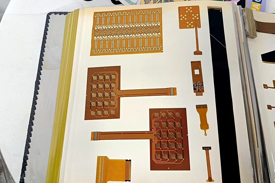
Quick Decision: PCB, FPC, or Printed PET?
The shortest defensible answer is to select the circuit by the constraint the interface cannot negotiate away. PCB supplies rigidity and a familiar PCBA process. FPC supplies bendable copper interconnect. Printed PET supplies a thin additive circuit for comparatively simple switching. The table is a screening tool, not a substitute for the released stack drawing.
| Project condition | First platform to evaluate | Why | Boundary to check |
|---|---|---|---|
| Flat passive key matrix; modest route count | Printed PET | Screen-printed conductors can combine the circuit and tail on a thin film | Finished circuit resistance, crossover count, contact finish, and environmental exposure |
| Interface must support the electronics mechanically | Rigid PCB | FR-4 can act as the switch circuit and a structural electronics carrier | Enclosure depth, mounting strain, board thickness, and flatness |
| Soldered LEDs, drivers, protection, or logic sit behind the keys | Rigid PCB | Conventional SMT assembly and inspection fit naturally | Thermal profile, component keep-outs, dome clearances, and repair access |
| Copper traces must cross a fixed fold or curved routing path | FPC | Copper-on-polyimide can route through a designed bend zone | Stack-specific radius, copper type, layer count, coverlay, and installation strain |
| The tail moves repeatedly in service | Dynamic FPC design | Flex life can be engineered and tested | Motion envelope, cycle count, strain relief, and dynamic-flex qualification |
| Thin integral tail goes into a fine-pitch ZIF connector | FPC, or a qualified PET tail | Both may be possible; the connector and process capability set the answer | Pitch, tail thickness, stiffener, exposed-contact geometry, wear, and registration |
| Lowest resistance within a narrow tail | FPC copper, then PCB copper if rigidity is acceptable | Copper geometry usually reaches lower resistance than a comparable printed-ink route | Trace width, copper thickness, temperature rise, connector resistance, and return path |
| Lowest-complexity circuit with no soldered electronics | Printed PET | Copper fabrication and PCBA steps may add no useful function | Compare quotations on the same drawing, volume, tooling ownership, and test scope |
A PCB and FPC membrane switch build becomes relevant when the stack needs copper density, component assembly, or a controlled bend. That does not make copper an automatic upgrade. If a printed PET circuit passes the electrical and environmental requirements with margin, changing platforms can add cost and process steps without improving the finished product.
Define the Three Circuit Stacks Before Comparing Them
PCB, FPC, and printed PET describe the circuit carrier and conductor process—not the complete membrane switch. The overlay, spacer, dome or shorting contact, adhesive perimeter, backer, tail exit, and enclosure still determine tactile behavior and much of the environmental performance.
Rigid PCB-backed membrane switch
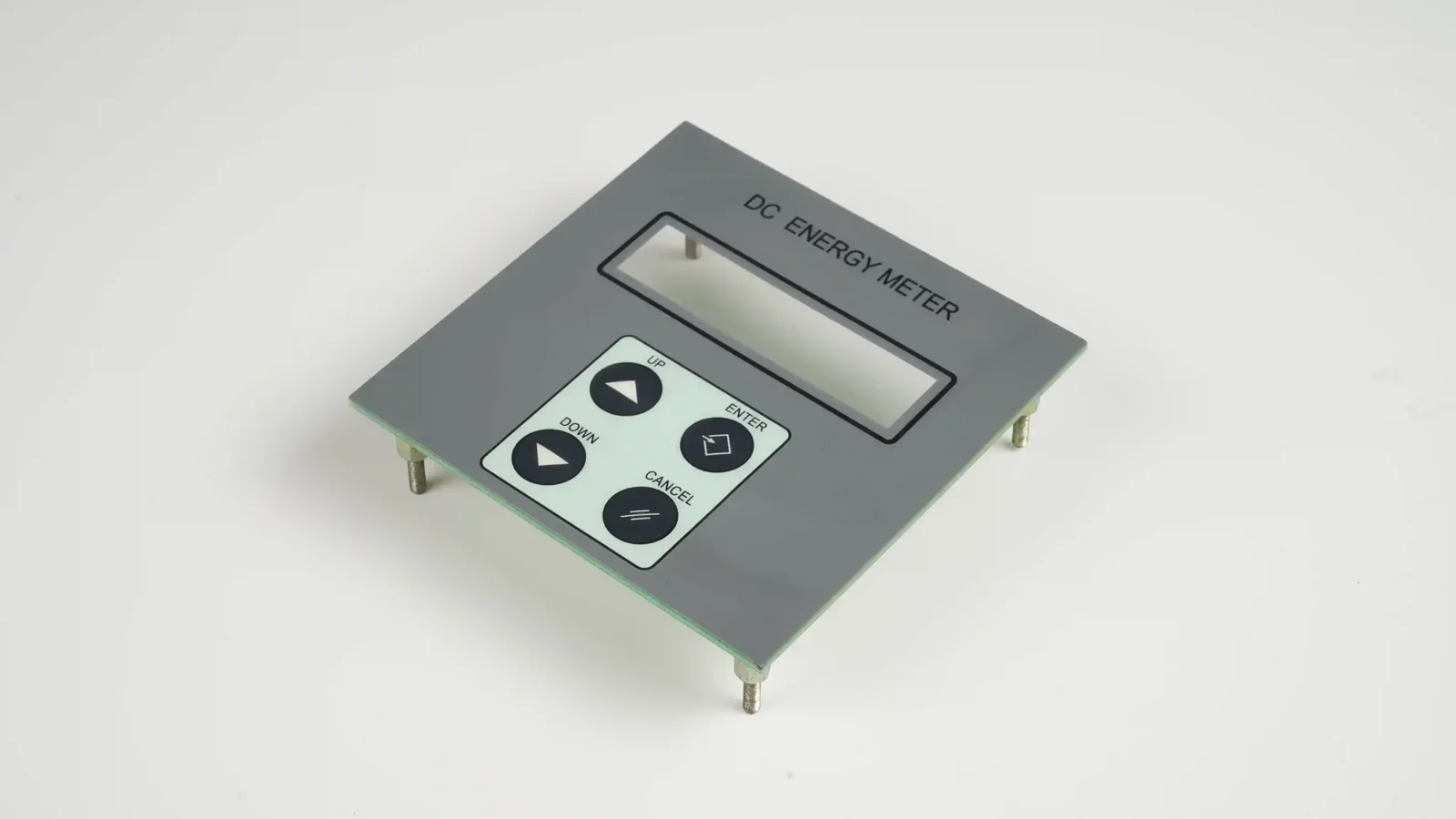
A PCB-backed membrane switch uses a rigid organic board, commonly an FR-4 construction, with etched and plated copper features. The board may carry switch contact pads on its front and soldered components or connectors elsewhere. IPC-6012F establishes qualification and performance requirements for finished rigid printed boards; the drawing still has to state the applicable design, class, material, finish, and acceptance requirements.
Graphic overlay
Adhesive / spacer / dome or shorting layer
Rigid PCB: copper pads + dielectric + optional multilayer routing
Optional SMT components and board-level connector
Enclosure bosses, fasteners, gasket, or backplate
The PCB is not the best choice when the interface must wrap around a housing, pass through a moving hinge, or remain label-thin and carries no electronics that justify a rigid carrier.
FPC membrane switch
An FPC membrane switch uses etched copper on a flexible dielectric, typically a polyimide-based laminate with coverlay and local stiffeners. DuPont’s Pyralux material guide describes the material family as copper-clad laminates, coverlays, bond plies, and bonding sheets. IPC-2223 governs flex and rigid-flex design, while IPC’s revision table identifies IPC-2223E as the active revision; confirm the contract revision at drawing release.
Graphic overlay
Adhesive / spacer / dome or shorting layer
Coverlay + copper + polyimide (+ more copper/dielectric layers if required)
Local stiffener under connector or components
Defined static or dynamic bend zone → controller connector
The FPC is not the best choice when the circuit needs to support switches or components as a rigid plate, or when a simple printed PET matrix already meets routing and resistance limits.
Printed PET circuit
A printed PET circuit deposits conductive silver, carbon, and dielectric materials onto a polyester film through additive printing and curing steps. MacDermid Alpha’s Autostat technical information lists heat-stabilized PET films for flexible circuits and membrane-switch layers, including common gauges of 75, 125, and 250 μm. Those gauges describe one material family, not a mandatory membrane-switch stack.
Graphic overlay
Adhesive / spacer / dome or printed shorting layer
Printed silver conductors on heat-stabilized PET
Optional printed carbon contacts and dielectric crossovers
Integral PET tail + contact finish / stiffener as specified
The printed PET circuit is not the best choice when long or narrow routes cannot meet resistance limits, when dense soldered electronics dominate the assembly, or when the tail must survive repeated motion that the exact ink-film system has not passed.
PCB vs FPC Membrane Switch Routing and Resistance
Routing capacity is a geometry problem before it is a platform label. Count the nets, reserve returns and shields, identify crossovers, set the tail width, and place component pads on the membrane-switch circuit drawing. Only then should the fabricator state achievable line/space, registration, conductor thickness, and electrical tolerance for the chosen process.
Use sheet resistance to compare conductors without hand-waving
For a uniform conductor, trace resistance can be estimated as:
Trace resistance = sheet resistance × (trace length ÷ trace width)
The length-to-width term is the number of “squares.” It makes unlike conductors comparable while exposing the assumptions.
The following values are public supplier examples, not JASPER manufacturing specifications or default build values. They show the level of material and connector detail that belongs in a comparison. A released project must use the selected material grade, finished geometry, supplier data sheet, and production measurements.
| Comparison input | Public supplier example | Source boundary |
|---|---|---|
| Copper conductor thickness | 35 μm (1 oz/ft²) | Pyralux AG lists 7 μm, 9 μm, 12 μm, 18 μm, and 35 μm copper options |
| Heat-stabilized PET substrate | 125 μm | MacDermid Alpha lists 75, 125, and 250 μm Autostat gauges |
| Cured printed-silver layer | 25 μm at ~7 mΩ/sq typical | Henkel LOCTITE ECI 1010 product-specific value |
| Fine-pitch tail reference | 0.5 mm ZIF pitch | TE Connectivity catalog example; final tail geometry follows the named connector |
These supplier examples do not replace IPC-2221C, IPC-2223E, IPC-6012F, IPC-6013E, or IPC-2152 design and acceptance requirements.
The conductor benchmark below uses the international annealed-copper resistivity reported in NIST/Bureau of Standards copper data and Henkel’s product-specific value for LOCTITE ECI 1010, a screen-printable silver ink.
| Conductor benchmark | Stated thickness | Sheet resistance at stated condition | 100 mm × 0.5 mm trace, calculated |
|---|---|---|---|
| Annealed-copper model | 18 μm | ~0.96 mΩ/sq | ~0.19 Ω |
| Annealed-copper model | 35 μm | ~0.49 mΩ/sq | ~0.10 Ω |
| LOCTITE ECI 1010 printed silver | 25 μm | ~7 mΩ/sq typical | ~1.40 Ω typical |
The table is a transparent materials benchmark, not a guaranteed PCB/FPC/PET ratio. Etch tolerance, copper type, plating and finish, cured ink thickness, ink lot, temperature, terminals, switch contacts, and connector resistance all move the finished measurement. The useful action is to put maximum end-to-end resistance on the drawing and verify it on first articles and production test coupons.
Do not copy a copper-current chart onto a printed PET circuit
IPC-2152 relates copper conductor size, current, and acceptable temperature rise in printed-board design. That framework is relevant to copper on PCB and FPC, but it does not establish the current rating of a polymer-thick-film silver trace on PET.
For printed PET, the engineer should calculate power loss = current² × resistance from the selected ink’s cured sheet resistance, then qualify the actual trace on the actual film, adhesive, enclosure, and duty cycle. For FPC, thin construction can limit heat spreading even when electrical resistance is low. For PCB, planes and a thicker board may spread heat more effectively, but enclosure temperature and component heating still matter. “Copper carries more current” is directionally useful; it is not a finished specification.
Component Support Changes the Assembly Process
Component count does more than add BOM lines; it chooses an attachment process, inspection method, strain-control strategy, and rework policy. A platform that can route a circuit may still be a poor host for the required package or thermal cycle.
PCB: the natural rigid electronics carrier
A PCB-backed membrane switch fits conventional SMT and through-hole workflows. It can place current-limiting resistors, protection devices, LED drivers, connectors, and logic on the same rigid carrier as the key contacts, subject to dome keep-outs, overlay height, and enclosure clearance. J-STD-001J and IPC-A-610J address soldering process/material requirements and post-assembly acceptability; neither standard proves the complete membrane switch will survive its application.
PCB loses its advantage when those components already live efficiently on the controller board. Duplicating electronics behind the overlay may complicate thermal management, repair, and configuration control.
FPC: soldered components need local mechanical control
FPC can carry soldered components, but a bendable laminate does not make every populated area bendable. The released design should keep component lands, via structures, and solder joints outside the intended bend, then define stiffener material, adhesive, outline, and transition geometry. The fabricator should review the complete stack to IPC-2223E design and IPC-6013E performance requirements at the revisions named in the procurement document.
An FPC is a poor component carrier when the assembly needs a broad rigid support surface, heavy connectors, field-replaceable modules, or frequent component rework. A rigid-flex or separate PCB may place rigidity exactly where it is useful.
Printed PET: attach is a qualified material system
Printed PET can host selected components through conductive adhesive or compatible low-temperature materials, but the ink, dielectric, film, pad geometry, cure, adhesive, and component termination must be qualified together. Sun Chemical’s printed-electronics portfolio describes silver/carbon conductors, dielectric systems, and materials for component attach on flexible substrates; that supplier scope does not authorize a generic PCB reflow profile on PET.
For a passive key matrix, “no components on the membrane” is often the cleanest architecture. When several drivers, protection devices, or connectors migrate onto the interface, a PCB/FPC HMI assembly may reduce interconnects—but only if the combined assembly remains inspectable and serviceable.
FPC Membrane Switch Comparison: Bend Requirements Separate FPC from “Flexible” PET
FPC should be selected for an engineered bend, while printed PET should be selected for a printed circuit that may conform within its qualified limits. Those are different requirements. “Flexible” does not say whether the tail is installed once, folded once, or moved through a million cycles.
| Bend case | PCB | FPC | Printed PET |
|---|---|---|---|
| Flat installation | Suitable | Suitable, but flex may be unnecessary | Suitable if electrical limits are met |
| One-time routing around a fixed feature | Not without a separate cable or flex section | Design a static bend zone | Possible only within supplier-qualified film/ink limits |
| Repeated service motion | Not a bendable carrier | Design and validate as dynamic flex | Do not assume suitability; validate the exact printed stack |
| Component located near the bend | Keep on rigid board | Move land/joint out of the bend and add transition control | Avoid placing an attach joint in the strain zone unless specifically qualified |
| Circuit must also support the panel | Strong candidate | Requires a backer or local stiffener | Requires a backer if structural support is needed |
The FPC drawing should name whether each bend is static or dynamic, show the installed path and neutral position, state the minimum inside radius, mark keep-outs, and identify stiffener edges. Radius cannot be copied safely from a generic article because copper type, thickness, layer count, adhesive system, coverlay, and bend direction all matter.
Printed PET needs the same discipline. IPC-9204 catalogs flexibility and stretchability tests for printed electronics, but IPC explicitly describes it as guidance rather than endorsement of a single test. The project should define its actual mandrel or motion path, temperature, cycle count, electrical monitoring, and failure criterion.
Connector Strategy Starts at the Receiving Connector
The host connector fixes more of the tail than the words PCB, FPC, or PET do. Pitch, contact side, mating thickness, exposed-contact length, stiffener, insertion direction, retention, and service access belong in the connector and tail drawing before the tail outline and conductor fan-out are frozen.
TE Connectivity, for example, publishes 0.5 mm-pitch ZIF FPC connector geometry and describes FPC connector families at 0.3 and 0.5 mm pitch. Those catalog values prove that fine-pitch connector systems exist; they do not prove a specific membrane-switch supplier can hold the tail registration, thickness, surface finish, and wear requirements.
| Interconnect strategy | Best fit | Drawing details that prevent surprises |
|---|---|---|
| Integral FPC tail into ZIF | Thin copper routing through a bend | Connector manufacturer/part number, pitch, contact side, tail thickness, stiffener, exposed length, bend keep-out |
| Integral printed PET tail | Simple matrix where the print process can hold geometry | Same connector details plus contact ink/finish, print registration, abrasion and mating-cycle criteria |
| PCB header or wire-to-board connector | Rigid board that also supports components | Header height, polarization, mating direction, harness strain relief, assembly access |
| PCB edge contact | Direct insertion of a rigid card edge | Board thickness, bevel, plating/finish, insertion depth, retention, keep-out |
| Rigid PCB with FPC tail | Components need rigidity but the interconnect must bend | Rigid-flex transition, stack, stiffener, bend zone, connector end, assembly sequence |
FPC usually offers the cleanest route into a fine-pitch connector ecosystem. Printed PET may still work when the converter proves capability. PCB is often better with a board connector or a hybrid flex tail. The correct answer is the construction that mates to the named connector with measurable margin—not the one whose marketing page lists the smallest pitch.
Tooling and Cost Must Be Compared on One Released Configuration
Printed PET often begins with fewer process families for a passive matrix, but “PET is cheapest” is not a quotation. Area, yield, layer/crossover count, circuit density, component content, finish, tooling ownership, inspection class, and change frequency can reverse a casual ranking.
| Cost driver | Printed PET circuit | FPC | Rigid PCB |
|---|---|---|---|
| Circuit formation | Screens, print passes, cure cycles, dielectric/crossover steps | Imaging, etching, coverlay, possible plating and vias | Imaging, etching, drilling, plating, solder mask, finish |
| Panel utilization | Film nesting and print registration | Flex panel nesting; irregular tails can consume area | Board panelization and route/V-score constraints |
| Components | Qualified adhesive or low-temperature attach, limited by system | SMT with flex-specific support and handling | Conventional SMT/through-hole options |
| Interconnect | Printed tail, crimp, or qualified ZIF contact | Integral flex tail and stiffener | Header, harness, edge contact, or added flex tail |
| Engineering change | New screens/artwork and possibly dies | New data, imaging, coverlay and tooling impacts | New board data; stencil, fixture, or assembly-program impacts |
| Test | Electrical fixture plus visual/registration checks | Bare-flex electrical/acceptance tests plus assembly tests | Bare-board and PCBA tests plus membrane-stack tests |
Request all three quotations from the same controlled package: outline, stack, netlist, tail and connector, BOM, annual and lot quantities, tooling ownership, inspection level, electrical limits, environmental plan, packaging, and change-control expectations. A PCB quote that includes populated electronics is not directly comparable to a bare printed PET matrix. Neither is an untested FPC quote comparable to a fully fixtured production test.
Failure Chains Reveal What the Platform Name Hides
Reliability becomes actionable when it is written as a chain from design input to physical damage to electrical symptom. The chain also identifies where to inspect and what to measure.
| Design or assembly error | Physical chain | Likely symptom | Prevention / evidence |
|---|---|---|---|
| Printed trace is too long or narrow for load | Higher resistance → current-squared heating → conductor/adhesive aging | Resistance drift, dim LEDs, intermittent or open circuit | Sheet-resistance calculation, thermal worst case, first-article resistance and post-stress measurement |
| FPC bends at a stiffener edge or populated land | Strain concentration → copper or joint fatigue | Motion-dependent intermittent, then open | Mark bend and keep-out zones; inspect installed path; run powered motion cycling |
| PCB is pulled flat by uneven bosses or fasteners | Board strain → pad, via, solder-joint, or contact distortion | Key variation or intermittent assembly fault | Flatness and mounting plan, controlled torque, strain/functional test in the production enclosure |
| Tail contact side, thickness, or stiffener is wrong | Partial connector engagement → high contact resistance or fretting | Intermittent tail, heat, field disconnect | Named connector, mating drawing, go/no-go geometry, contact resistance and mating-cycle test |
| Tail exit or adhesive perimeter is poorly designed | Ingress path → contamination/corrosion → leakage, short, or open | Environment-dependent false input or dead key | Enclosure-level ingress validation, edge-seal inspection, pre/post-stress insulation and functional test |
Notice what is absent: no row says “PET fails,” “FPC fails,” or “PCB is reliable.” Each platform has controllable interfaces. A sealed overlay does not rescue an undefined tail exit, and a Class 3 flex callout does not rescue a component placed in the bend.
Validate the Assembly, Not Just the Bare Circuit
A useful approval plan links each risk to a sample, condition, measurement, and pass/fail limit. IPC-9257 says electrical testing of flexible printed electronics verifies network connectivity but does not establish geometry, registration, assembly suitability, or every customer requirement. The validation matrix must therefore extend beyond continuity.
Assign each standard to the correct deliverable
IPC revisions can change after an article is published. The procurement team must confirm the current edition and the contract revision at drawing release.
| Document | Published revision/date shown by IPC | What it controls in this comparison |
|---|---|---|
| IPC-2221C | 2023 | Generic printed-board design inputs used with the sectional standard |
| IPC-2223E | 2020 | Flexible and rigid-flex design, including interconnect and component-mounting structures |
| IPC-6012F | 2023 | Qualification and performance of finished rigid printed boards |
| IPC-6013E | 2021 | Qualification and performance of finished flexible and rigid-flex printed boards |
| IPC-2152 | 2009 | Copper conductor size, current, and acceptable temperature-rise relationship |
| IPC-6902 | 2021 | Qualification and performance of printed electronics on flexible substrates |
| IPC-9257 | 2021 | Electrical-test selection for flexible printed electronics |
| J-STD-001J / IPC-A-610J | 2024 | Soldering process/material requirements and post-assembly acceptability |
| IPC-9204 | 2017 | Non-mandatory flexibility/stretchability test guidance for printed electronics |
IPC listed IPC-2223F and IPC-6013F as draft work at the cutoff, not as permission to cite an unreleased revision. The drawing should name the adopted document and revision instead of saying only “built to IPC.”
The cutoff therefore separates 2026 research from 2024 assembly documents, 2023 rigid-board documents, 2021 flex-performance and electrical-test documents, and 2020 flex-design documents.
| Approval item | All constructions | Extra focus by platform | Required output |
|---|---|---|---|
| Drawing and stack audit | Outline, key centers, spacer vents, adhesive perimeter, tail exit, connector | PCB mounting/flatness; FPC bend/stiffener; PET ink/dielectric/contact system | Signed drawing and controlled BOM |
| Dimensional inspection | Critical-to-function dimensions and registration | Tail width/thickness, exposed contact length, contact side | First-article report with actual values |
| Electrical network test | Opens, shorts, pinout, end-to-end resistance | PET resistance distribution; FPC/PCB via and multilayer nets | Netlist-based report and limit table |
| Component attach | Function, polarity, workmanship, repair policy | J-STD-001J/IPC-A-610J for soldered builds; project criteria for printed PET attach | Inspection record and functional result |
| Connector test | Mating, retention, contact resistance, strain relief | Wear/contact finish on PET; stiffener transition on FPC; harness load on PCB | Named connector and cycle/retention result |
| Mechanical fit | Install in production-intent enclosure | Fastener strain on PCB; static/dynamic path on FPC; crease avoidance on PET | Fit photos, measured clearances, functional test while mounted |
| Environmental stress | Temperature/humidity, chemicals, vibration/shock, and ingress only as required by the end use | Monitor the platform-specific failure chain during and after stress | Pre/post resistance, insulation, appearance, and function |
| Tactile and endurance | Force/travel, contact behavior, key cycling | Hold overlay, spacer, dome, backer, and mounting constant when comparing circuits | Sample plan, cycle profile, failure definition, raw results |
Many historical F01.18 membrane-switch methods were withdrawn in 2023 or 2024. A drawing should not copy a familiar ASTM F-number from an old design guide without checking status. Define the method directly, or name a current standard and revision that matches the end product. The quality and testing plan should also state whether samples are destructive and whether stressed units may ship.
Decision Matrix: Choose the Circuit Platform for the Stack
The final PCB vs FPC membrane switch choice should come from the dominant constraint, then be challenged by the “not best when” column. Printed PET remains in the matrix because it is often the correct reference architecture.
| Dominant requirement | Recommended starting point | Not the best choice when… |
|---|---|---|
| Rigid support plus populated electronics | PCB-backed membrane switch | The housing is curved, depth is tight, or the circuit must move |
| Thin copper routing through a fixed bend | FPC membrane switch | The flex is being asked to act as a structural plate |
| Repeated controlled motion | Dynamic FPC construction | The motion path, cycle count, radius, and strain relief cannot be defined or tested |
| Simple low-current switch matrix | Printed PET circuit | Resistance, routing density, component attach, or environmental limits lack margin |
| Fine-pitch ZIF tail | FPC first; qualified PET as an alternative | The receiving connector is not yet selected |
| Components on a rigid island plus a flexible tail | Rigid-flex or PCB-plus-FPC hybrid | A standard board and separate inexpensive tail already meet reliability and service goals |
| Lowest total cost | Quote all viable platforms on one release package | Quotes differ in BOM, test, tooling ownership, or acceptance scope |
Before tooling, release a one-page circuit-platform input sheet containing:
- Panel outline, key centers, backer, mounting method, and depth budget.
- Schematic/netlist, route count, return/shield needs, and maximum end-to-end resistance.
- Voltage, continuous and peak current, duty cycle, allowable temperature rise, and ambient range.
- Component BOM, package sizes, side of assembly, height limits, and service/rework policy.
- Receiving connector manufacturer and part number, pinout, contact side, pitch, and mating direction.
- Tail length, exit, thickness, exposed contacts, stiffener, strain relief, and installed path.
- Every static bend and dynamic motion zone, including radius, direction, cycle count, and keep-outs.
- Environmental exposures, ingress boundary, cleaning agents, vibration/shock profile, and application-specific standards.
- Required IPC document numbers, revisions, performance class where applicable, and any customer acceptance criteria.
- Prototype quantity, production lot/annual volume, tooling ownership, change control, traceability, and sample-approval tests.
JASPER’s public scope includes PCB-backed, FPC, and hybrid membrane-switch builds and review of stack-up, bend zones, routing, connectors, and test inputs. That makes JASPER one manufacturer option for the construction review, not evidence that a platform is prequalified for a particular product. Compare JASPER and alternative fabricators against the same input sheet, require actual capability data, and approve the stack through production-intent samples. A project team can send that input sheet for an engineering review before tooling.
Frequently Asked Questions
What decides a PCB vs FPC membrane switch choice?
Choose PCB when the interface needs rigidity, conventional populated-board assembly, or board-level connectors. Choose FPC when copper routing must pass through a defined bend. If neither constraint exists, compare both against printed PET rather than assuming copper adds value. The released geometry and validation plan make the final decision.
When is a printed PET circuit the best option?
A printed PET circuit is a strong starting point for a thin, passive, low-current key matrix with modest routing density and limited component attach. It remains the right option only when the selected ink, film, contacts, tail, resistance limits, and environmental tests pass with adequate production margin.
Is a PCB backed membrane switch more reliable than FPC?
Not by platform name alone. PCB removes flex strain and provides rigid component support, while FPC removes separate wiring across a bend. Either can fail at joints, connectors, mounting points, or seals. Reliability must be stated as specific failure modes, operating conditions, test methods, sample sizes, and acceptance limits.
How much current can PCB, FPC, and printed PET traces carry?
There is no universal current rating. For PCB and FPC copper, size the conductor and acceptable temperature rise using the applicable copper-design method and actual thermal boundary. For printed PET, use the chosen ink’s cured sheet resistance, calculate current-squared power loss, and test production-representative traces, contacts, adhesive, and enclosure.
Can FPC and printed PET tails use a 0.5 mm ZIF connector?
FPC commonly mates to 0.5 mm ZIF families. Printed PET may also do so if the converter can control pitch, registration, tail thickness, contact finish, exposed length, stiffener, and wear. Name the connector part number first; then require a mating drawing, dimensional report, contact-resistance result, and cycle test.
Can SMT components be mounted on all three circuit types?
PCB and properly designed FPC support soldered SMT processes, with FPC requiring stiffened component zones outside intended bends. Printed PET can accept selected components through a compatible conductive-adhesive or low-temperature material system. Do not apply a generic reflow profile or workmanship criterion across all three; qualify the exact stack and attachment process.
Which IPC standards apply to these membrane-switch circuits?
Typical references include IPC-2221 and IPC-6012 for rigid boards, IPC-2223 and IPC-6013 for flex or rigid-flex, IPC-2152 for copper current/temperature-rise design, IPC-6902 and IPC-9257 for flexible printed electronics, and J-STD-001 with IPC-A-610 for soldered assembly. State the required revision on the drawing.
Can one membrane switch assembly use both PCB and FPC?
Yes. A rigid-flex construction or a rigid PCB with an attached FPC tail can keep components and connectors on a supported island while routing through a thin bend. It is not automatically better than a separate cable. Compare transitions, connector count, serviceability, panel utilization, assembly sequence, inspection, and replacement cost.
Freeze the circuit stack before tooling
Send the outline, stack, netlist, current and resistance limits, component BOM, named connector, installed tail path, bend zones, enclosure section, and validation plan. JASPER Engineering will identify unresolved PCB, FPC, printed-PET, connector, and test decisions before samples are released.