
Start with the disturbance and current-return path, not a shield material name. Coverage, aperture geometry, tail routing, enclosure contact, host protection, and production-equipment immunity tests must work as one system.
JASPER certifications: ISO 9001, ISO 13485, IATF 16949, and ISO 14001.
1. Start Membrane Switch EMI Shielding With the Disturbance
Start with a named source, coupling path, vulnerable circuit, and unacceptable response. “Add a shield” is not testable: an operator discharge, an RF field, and a burst on a control cable need different countermeasures.
That distinction matters in an industrial-control application near contactors, variable-frequency drives, radios, long cables, or dry-air operator stations. The switch face is only one entry surface; a cable, window, seam, mounting stud, or host PCB can dominate the result.
| Disturbance to evaluate | Likely coupling path | Failure to monitor | Design response to investigate | Test-family boundary |
|---|---|---|---|---|
| Operator ESD at key, window, bezel, or screw | Arc, flashover, capacitive coupling | False input, reset, lockup, damage | Dielectric, guard, discharge route, PCB entry protection | IEC 61000-4-2:2025 is equipment-level; it does not certify a shield layer. |
| Non-proximate radiated RF | Field coupling into loop, tail, cable, aperture | Key, display, analog, or data error | Coverage, termination, loop control, enclosure, filter | IEC 61000-4-3:2020 covers RF sources not close to the EUT. |
| RF on a conducting tail or cable | Common-mode current on signal, supply, shield, or ground | Repeated false input or data error | Tail, connector, reference plane, filter | IEC 61000-4-6:2023 publishes 150 kHz–80 MHz and requires a conducting path. |
| EFT/burst from switching | Applicable supply, signal, control, or earth port | Upset, state loss, reset, damage | Port classification, filter, protection, separation | IEC 61000-4-4:2012 is not an ESD test. |
| Internal emissions | Clock, converter, display, cable, aperture | Emissions failure or receiver interference | Source, return, enclosure, cable treatment | For vehicles, CISPR 25:2021 is emissions, not immunity. |
ESD is a short event from accumulated charge; EMI is the unwanted effect of radiated or conducted electromagnetic energy. A carbon guard may bleed charge yet do little against RF. Foil may cover the face yet fail through a long, narrow return.
Keep three labels distinct: protective earth serves safety, chassis or functional ground provides an equipment reference, and circuit 0 V returns electronics current. Their connection belongs to the system architecture. Calling all three “GND” leaves the interface undecided.
Material selection comes only after the disturbance and reference path are defined. No default voltage level, field strength, ground topology, or compliance result is assumed.
2. Put the Shield in a Complete Stack and Current Path
A complete stack controls the arc path, intercepts energy, and carries it to a defined reference. Layer order depends on actuation, windows, circuit, enclosure, and access. In PCB and FPC membrane switches, the tail transition matters as much as the face. This is a planning model, not a universal bill of materials.
Operator touch / external RF field
Graphic overlay and window system · dielectric + user interface
Optional shield · silver grid/solid print, carbon,
metallized film, foil, or clear layer
Dielectric isolation · prevents shield-to-signal contact
Upper circuit / dome retainer / components
Spacer and lower circuit
Rear adhesive, backer, or enclosure surface
shield path · signal path
tab / dedicated tail / · flex tail → connector →
connector pin / wrap bond host protection and input circuit
chassis or approved reference interface
Published membrane-switch design guides document carbon, silver, foil, metallized-polyester, solid/grid silver, separate-tail, shared-connector, and chassis-tab shield constructions. These are feasible forms, not pass results.
Separate three paths on the drawing
Shield path: coverage, keepouts, exit, contact, exposed bond, and destination reference.
Signal path: switch contact, pinout, tail, connector, filter, and transient protection.
Flashover path: surfaces, edges, windows, fasteners, adhesive gaps, and tail exit. Include the finished bezel and backer.
The common failure chain is short:
strike or RF field → incomplete coverage or high-impedance return → voltage develops across the shield/interface → energy couples into switch input/output lines or the host board → false actuation, reset, lockup, data error, or damage
Break the chain with the measure that controls its actual path: shield, dielectric, tail, seam, connector, PCB protection, or source suppression.
3. Choose the Printed Shield Layer, Foil, or Clear Conductor
Choose the least complex construction that controls the identified path without creating an optical, flex, bonding, or grounding problem. Sheet resistance matters; coverage, apertures, cure, adhesive conductivity, corrosion, and disturbance frequency matter too.
| Construction | Good fit | What it does not solve by itself | Evidence to put in the material file |
|---|---|---|---|
| Printed silver grid | Thin PET artwork, keepouts, routed guard | Open grid, narrow exit, poor cure, cable noise | Exact ink, thickness, Ω/sq method, grid, cure, ground exit |
| Solid printed silver | More coverage where opacity and ink use are acceptable | Host protection, enclosure bond, transparent window | Grid controls plus flex region, isolation, inspection |
| Printed carbon | Static bleed or ESD guard at higher sheet resistance | Metal-class low-impedance RF path | Carbon grade, Ω/sq, thickness, cure, humidity condition |
| Metal foil or metallized film | Nearly continuous metal coverage, direct chassis tab | Tight fold, window, seam, nonconductive adhesive | Alloy, thickness, carrier, adhesive, bond area, corrosion, bend limit |
| Transparent conductor or mesh | Display or indicator window | Haze, moiré, bus bar, frame gap | Ω/sq, transmission, haze, geometry, bond method |
Supplier numbers are inputs, not finished-switch claims
The Henkel EDAG 427 SS datasheet lists membrane switches and RFI shielding, reporting less than 0.075 Ω/sq at 25 µm for that silver ink. The Henkel EDAG 423SS carbon datasheet lists membrane switches and ESD protection, with results in the tens of ohms per square at 25 µm under stated PET and cure conditions. “Conductive ink” is not a specification.
Public supplier example: Henkel reports ≤0.075 Ω/sq at 25 µm cured thickness for EDAG 427 SS under its stated test conditions. Use that number only to understand the order of magnitude available from one named ink system. It is not a JASPER test result, a universal shield requirement, or a released acceptance value.
The 3M 1181 copper-foil TDS reports 0.066 ± 0.005 mm total thickness, 0.005 Ω/in² maximum resistance under a named method, and average 66 dB from 300 kHz to 2.5 GHz under ASTM D4935. Those are supplier-specimen results, not membrane-switch or JASPER attenuation. The 3M 1194 TDS makes a different trap explicit: its nonconductive adhesive does not drain static through the adhesive to ground. A copper backing alone proves no installed current path.
Use a grid only after defining what can pass through it
A grid saves conductive area but creates apertures. Define pitch, line width, sheet resistance, exit geometry, and permitted coupled voltage from the project, then test representative hardware. No source supports one universal grid pitch.
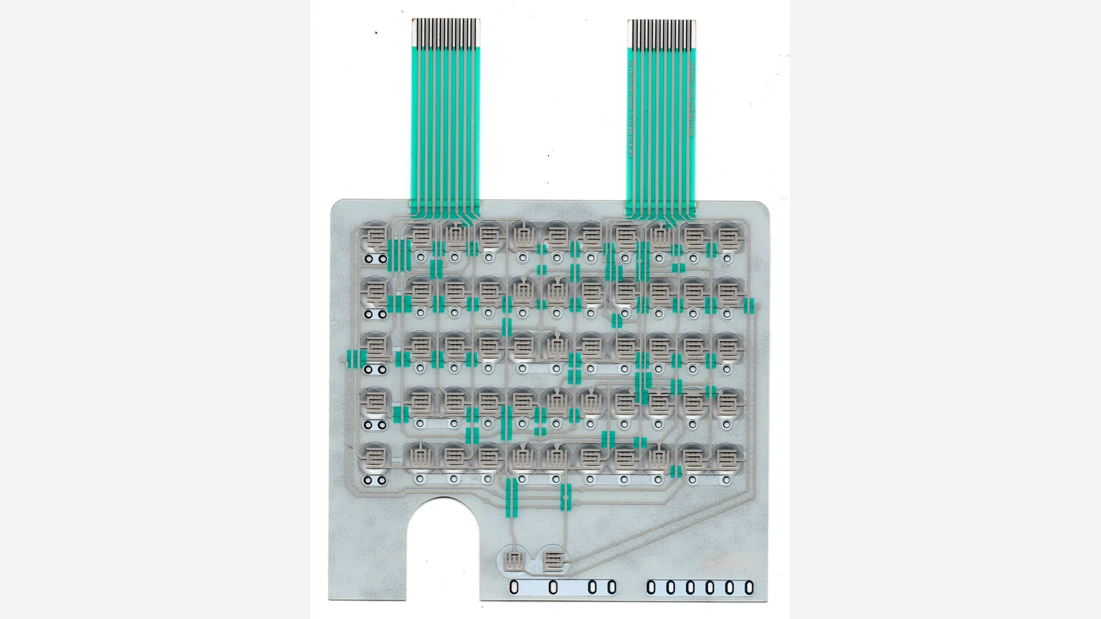
4. Design Membrane Keypad Grounding as a System Path
Membrane keypad grounding joins the switch, connector, PCB, enclosure, power architecture, and safety design. Name the destination node. IEC TR 61000-5-2 treats earthing and cabling as system-level EMC work; “ground shield” is incomplete because chassis, protective earth, circuit 0 V, cable shield, and an isolated reference need not be the same conductor.
| Termination | Use it when | Main risk to resolve | Drawing evidence |
|---|---|---|---|
| Perimeter / wrap bond | Conductive enclosure contacts a broad edge | Coating, seam, compression, corrosion | Perimeter, finish, gasket/adhesive, stops, fasteners |
| Multiple short tabs | Full perimeter bond is impractical | Unequal contact, current crowding | Count, width, length, landing, inspection |
| Dedicated shield tail | Shield stays separate to a defined node | Inductance, fatigue, routing beside input/output traces | Geometry, bend, pin, connector, host landing |
| Connector shield pin | One connector simplifies assembly | Common impedance and crosstalk | Pin adjacency, host route, plane, protection |
| Conductive adhesive / gasket | Low-profile enclosure bond | Contamination, coating, aging, compression | Material, substrates, area, pressure, environment |
Short and wide is an impedance rule
A continuity buzzer injects a small, slow current. ESD and RF do not. The Texas Instruments ESD report explains that high-frequency return current follows the lowest-impedance route and that larger loop area increases coupling. A near-zero DC reading can hide a long, narrow, or slotted transient path.
General Label prefers perimeter contact, then multiple short, wide tabs, and offers 3:1 maximum length-to-width as a single-tab heuristic. It is not a compliance threshold; enclosure, frequency, joint, loop, and EUT still decide the result.
Specify the joint, not just the conductive adhesive
The 3M Tape 9713 TDS reports less than 0.5 Ω for copper/copper and less than 2.5 Ω for aluminum/aluminum on prepared 1 × 1 in joints. 3M calls the data typical. Material, oxide, coating, area, pressure, preparation, environment, and aging still need acceptance controls.
Do not connect the shield to circuit 0 V merely because it is nearby. The approved EMC and safety architecture must decide before pinout release.
5. Route the Tail and Enclosure Contact Before Freezing the Pinout
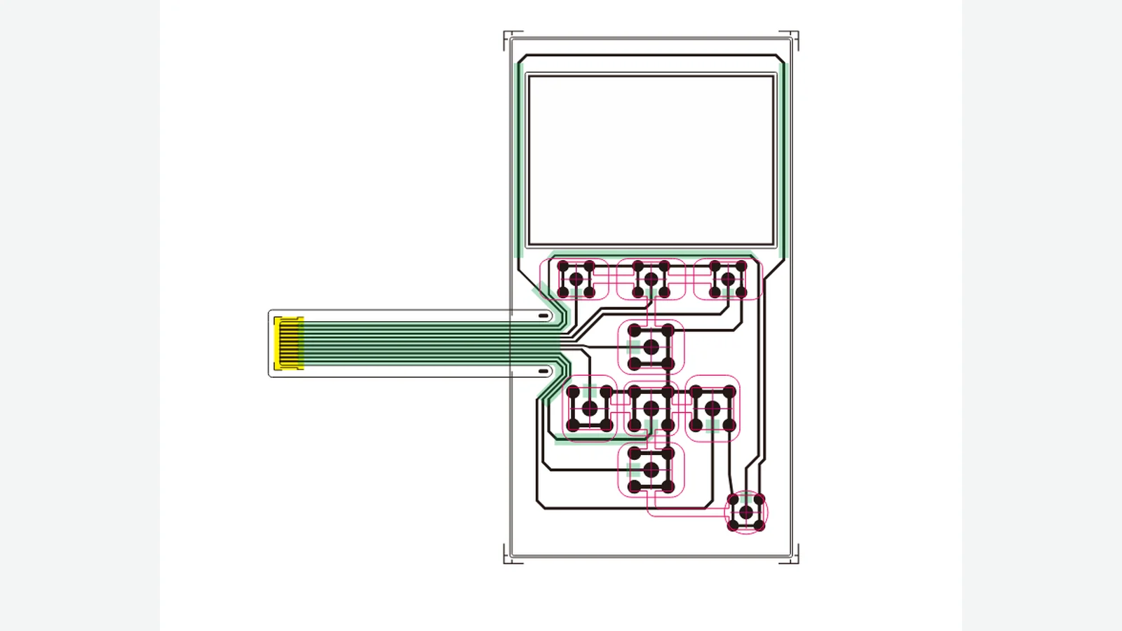
Tail routing can undo the shield because its conductor shares a small geometry with switch, LED, supply, and host-input lines. Solve the transition in the circuit and tail layout, before tooling.
Use this path review from the face toward the electronics:
- Intercept: cover keys, windows, edges, fasteners, and tail exit.
- Collect: merge the grid into a wide bus or expose qualified foil.
- Transfer: define tab, clamp, adhesive, wrap bond, or tail conductor.
- Reference: land at the approved node with a short loop.
- Protect: place required host protection at the entry.
- Route onward: separate protected signals from the ingress region.
The Texas Instruments layout guide places protection near the connector, minimizes ground-path inductance, and keeps unprotected circuits outside the ingress-to-protection region. Applied here, that is a system inference: a switch shield does not clamp every host input.
Treat the enclosure landing as a controlled joint
Coating, residue, oxide, or contamination can isolate a metal landing. Specify finish/mask, area, pressure, flatness, fastener or compression control, and inspection.
For a conductive gasket, compression is a design variable. The Parker Chomerics handbook gives profile-specific deflection bands. The enclosure needs a stop and tolerance analysis; “add conductive gasket” is not a drawing.
Prototype the real bend, tail length, connector, coating and fastener stack. A flat bench coupon with a temporary ground clip can screen material continuity; it cannot reproduce the production current path.
6. Know When an Added Shield Is Not the Best Choice
An added shield brings another layer, dielectric interface, termination, and inspection path. Use it when the documented coupling path crosses the switch, not as insurance against an unnamed risk.
| Project condition | Why the obvious shield choice can fail | Better first investigation |
|---|---|---|
| EUT already passes with margin | A new floating layer adds a path without fixing a problem | Preserve and document the tested stack |
| Noise enters by cable or connector | Face shield misses common-mode current and PCB entry | Cable/connector bond, common-mode control, PCB protection |
| Window occupies the exposed area | Opaque foil blocks it | Clear conductor, mesh, frame, smaller aperture |
| Tail bends or folds tightly | Foil concentrates strain | Printed/segmented shield, new exit, enclosure bond |
| No approved reference exists | Long route to 0 V may inject noise | Isolation, dielectric, guard, ground architecture |
| RF returns through one narrow tail | Low DC resistance hides inductance and loop area | Perimeter or multiple bonds, backer, enclosure redesign |
A printed silver grid is not the best choice when solid coverage, a very low-impedance perimeter bond, or a shielded window is needed and the grid cannot meet the system test. Foil is not the best choice when opacity, fold life, added thickness, edge handling, or a nonconductive adhesive defeats the assembly. Carbon is not the best choice when the requirement is metal-class RF shielding rather than static bleed.
“No added shield” also needs a recorded stack, environment, EUT, test, severity, criteria, and margin.
7. Prepare the Immunity Test Plan Before Drawing Release
The test plan should identify the finished equipment standard first, then select the applicable basic methods, ports, severity, setup, operating modes, monitoring, and performance criteria. A membrane switch has no universal “IEC level.” The applicable product standard, customer/OEM specification, or approved laboratory plan supplies that requirement.
IEC 61000-6-2:2016 is a generic industrial immunity standard only when no relevant dedicated product or product-family standard exists. IEC 61326-1:2020, for example, covers applicable measurement, control, and laboratory equipment. Automotive projects may use ISO and CISPR routes instead. Standards selection belongs to the finished-product compliance owner.
| Phenomenon | Current reference and scope boundary | Representative EUT and interface | Monitor during exposure |
|---|---|---|---|
| Operator and nearby-object ESD | IEC 61000-4-2:2025; equipment-level immunity, not shield-coupon certification | Powered HMI with production overlay, keys, windows, bezel, fasteners, shield, real ground point, tail, connector and host electronics | False or missed actuation, reset, lockup, data error, permanent change and required recovery action |
| Non-proximate radiated RF | IEC 61000-4-3:2020; RF fields from sources not close to the EUT | Powered EUT with representative enclosure, cable set, tail length, termination and operating mode | Key state, display, communications, analog values, faults and recovery |
| EFT/burst | IEC 61000-4-4:2012; applicable supply, signal, control and earth ports | Ports classified by the governing standard, with production cable and connector configuration | Momentary upset, state loss, reset, communication error, damage |
| Surge | IEC 61000-4-5:2014+A1:2017; switching and lightning-related unidirectional surges | Exposed power or long-interconnect port only when installation and the governing standard make it applicable | Protection operation, interruption, recovery and permanent damage |
| Conducted RF | IEC 61000-4-6:2023; public scope 150 kHz–80 MHz and a conducting coupling path | Relevant supply, signal, shield or ground conductor with real routing and termination | False input, threshold shift, communication error and recovery |
| Automotive ESD | ISO 10605:2023; module-bench and complete-vehicle ESD from assembly, service and occupants | Production-representative module, harness, panel, enclosure and ground; vehicle test when the OEM plan requires it | OEM-defined functional status, resets, unintended commands and recovery |
| Automotive emissions companion | CISPR 25:2021; vehicle radio-disturbance emissions, not immunity | Vehicle or component/module with representative harness and receiver-protection context | Emissions result under the applicable method; do not put it in the immunity pass/fail column |
Public catalog pages establish scope and edition, not the full test table. Use the controlled standard and project specification for severity, setup, exposures, operating modes, and acceptance criteria.
Use four evidence gates
- Material/process: verify grade, cure, thickness, sheet resistance, registration, adhesion, and isolation.
- Switch assembly: inspect coverage, shorts, resistance map, pinout, and the production-equivalent layer stack and enclosure joint.
- Integrated pre-compliance: power representative hardware with production firmware, cables, enclosure, ground, and monitoring.
- Formal equipment: run the approved plan and retain the configuration, deviations, result, and tested revision.
JASPER's testing and quality workflow can support switch-level checks. It does not prove an unspecified design passes an IEC, ISO, CISPR, regulatory, or customer requirement.
Retire a legacy ASTM shortcut
ASTM's electronics standards list marks F1812-15 withdrawn in 2024. If a legacy contract still cites it, document that status and do not substitute it for the applicable equipment standard.
Continuity and sheet-resistance checks are diagnostics, not immunity evidence. That requires a representative EUT under approved conditions.
8. Release a Drawing and Sample-Approval Package That Can Be Tested
A useful drawing links environment, stack, termination, and acceptance. “ESD shield required” does not.
Six-step engineering and sourcing process
- Classify: product, installation, contact, sources, cables, environment, service.
- Freeze tests: standard/edition, overlay, ports, severity, points, modes, criteria.
- Map: source, entry path, shield/barrier, return, protected victim.
- Release: materials, stack, artwork, dielectric, tail, connector, enclosure, reference diagram.
- Approve: TDS revision, dimensions, cure, sheet resistance, continuity, isolation, pinout, bond.
- Integrate: correlate switch checks, pre-compliance, formal results, and drawing revision.
| Required project input | What to provide | Decision it controls |
|---|---|---|
| Product and use environment | Equipment type, installation, operator access, service and nearby sources | Applicable standard, exposure points and material environment |
| Standard basis | Standard number, edition, customer/OEM document and deviations | Test method, severity, setup and evidence package |
| Performance criteria | Allowed degradation, prohibited response, recovery and permanent-damage rule | Firmware monitor and pass/fail decision |
| Exposed geometry | Overlay, windows, bezel, screws, seams, cutouts, tail exit and backer | Dielectric distance, edge guard and shield coverage |
| Ground architecture | Protective earth, chassis, functional ground, circuit 0 V and intentional connections | Shield endpoint and connector/PCB transition |
| Shield construction | Ink/foil/film family, coverage, grid or solid artwork, keepouts and dielectric isolation | Electrical path, optical effect, stack height and inspection |
| Material evidence | Supplier, exact grade, TDS revision, cured thickness, sheet resistance and cure | Process window and incoming acceptance |
| Tail and connector | Length, bends, pinout, mating part, shield pin/tab and host landing | Path impedance, crosstalk, assembly access and serviceability |
| Enclosure joint | Material, finish, masked area, gasket/adhesive, pressure, fasteners and tolerances | Contact resistance, corrosion, compression and repeatability |
| Host protection | Input topology, protection device, filter, reference plane and placement | Residual energy at the vulnerable electronics |
| Representative EUT | Hardware, firmware, cable set, load, enclosure and operating states | Whether pre-compliance matches production intent |
| Approval records | First-article report, resistance map, isolation test, photos, EUT log and revision IDs | Traceability from material lot to formal test report |
Release blockers include unspecified conductive adhesive, foil without contact detail, shield pin without host landing, painted chassis pad, undefined ground node, grid without geometry, unsourced test level, or supplier attenuation copied as equipment performance.
Request design and DFM review before release if the enclosure, ground node, window, tail, or test basis is moving. Review cannot replace testing; it can prevent an untestable interface.
9. Frequently Asked Questions
What is membrane switch EMI shielding?
Membrane switch EMI shielding is a conductive layer and termination designed to control electromagnetic energy that could couple into or out of the switch and its tail. The construction may use printed silver, carbon, metallized film, metal foil, mesh, or a transparent conductor. Its effectiveness depends on the complete equipment path, not the layer alone.
How is membrane switch ESD protection different from EMI shielding?
Membrane switch ESD protection manages short discharge events from accumulated static charge, while EMI shielding addresses unwanted electromagnetic coupling that may be radiated or conducted. One construction can contribute to both, but the current path, bandwidth, dielectric spacing, host protection, and test method differ. The terms should not be treated as interchangeable requirements.
Which printed shield layer is best for a membrane switch?
No printed shield layer is best for every project. Silver offers a lower-resistance printed path than typical carbon; carbon can suit static bleed; solid print closes grid apertures; foil offers continuous metal coverage; and transparent conductors preserve windows. Choose from the disturbance, required coverage, flex, optics, termination, material data, and representative EUT testing.
Must a membrane switch shield always be grounded?
A conductive shield needs an intentional electrical role and reference, but “grounded” is not a complete instruction. The design may bond to chassis, functional ground, circuit 0 V, a cable-shield structure, or another approved reference. A floating layer may behave unpredictably. The finished-equipment EMC and safety architecture must define the endpoint and connection method.
Can membrane keypad grounding share circuit 0 V?
Membrane keypad grounding can share circuit 0 V only when the approved equipment architecture calls for that connection. Direct bonding may work in one design and inject disturbance into sensitive electronics in another. Define protective earth, chassis, functional ground, cable shield, and circuit 0 V separately, then document any direct, capacitive, resistive, or isolated relationship.
Is a silver grid better than metal foil for EMI shielding?
A silver grid is better when low thickness, flexible artwork, tailored keepouts, and integrated printing outweigh the loss of solid coverage. Metal foil is better when continuous low-resistance coverage and a broad bond are feasible. Neither wins if the ground path, window, edge, adhesive, connector, or enclosure creates the dominant coupling path.
Which EMC standards apply to a shielded membrane switch?
The finished product determines the applicable standards. Common methods include IEC 61000-4-2:2025 for equipment ESD, IEC 61000-4-3:2020 for non-proximate radiated RF, IEC 61000-4-4:2012 for EFT/burst, and IEC 61000-4-6:2023 for conducted RF. Industrial, automotive, medical, or other product-family standards can add or replace requirements.
Can continuity or sheet resistance prove EMC compliance?
No. Continuity and sheet resistance are useful material and assembly diagnostics, but they do not reproduce the production enclosure, current-return impedance, cable coupling, host electronics, firmware, operating mode, or performance criteria. Compliance requires a representative finished EUT tested under the applicable standard and an approved, documented configuration.
10. Share the Electrical Environment and Grounding Points
Send the equipment type, disturbance sources, governing standard and edition, test severity, exposed points, prohibited responses, overlay/window geometry, enclosure material and finish, ground-reference diagram, tail route, connector, host protection, and representative cable set. That package lets the switch and equipment teams review one current path instead of separate parts.
JASPER is one membrane-switch manufacturer that can review the stack, artwork, tail, connector and enclosure interface from those inputs. The review should produce a testable drawing and first-article plan, not an unqualified compliance promise. Formal acceptance still belongs to the production-representative equipment and its approved laboratory program.
Define the current path before choosing the shield
Send the disturbance sources, test standard and severity, exposed points, enclosure finish, ground-reference diagram, tail route, connector, host protection, and representative cable set for one joined review.