
LED integration is one controlled chain from controller limits and a named LED part through branch routing, pocket geometry, optical masking, enclosure effects, and a powered first article. Freeze each input before releasing the circuit.
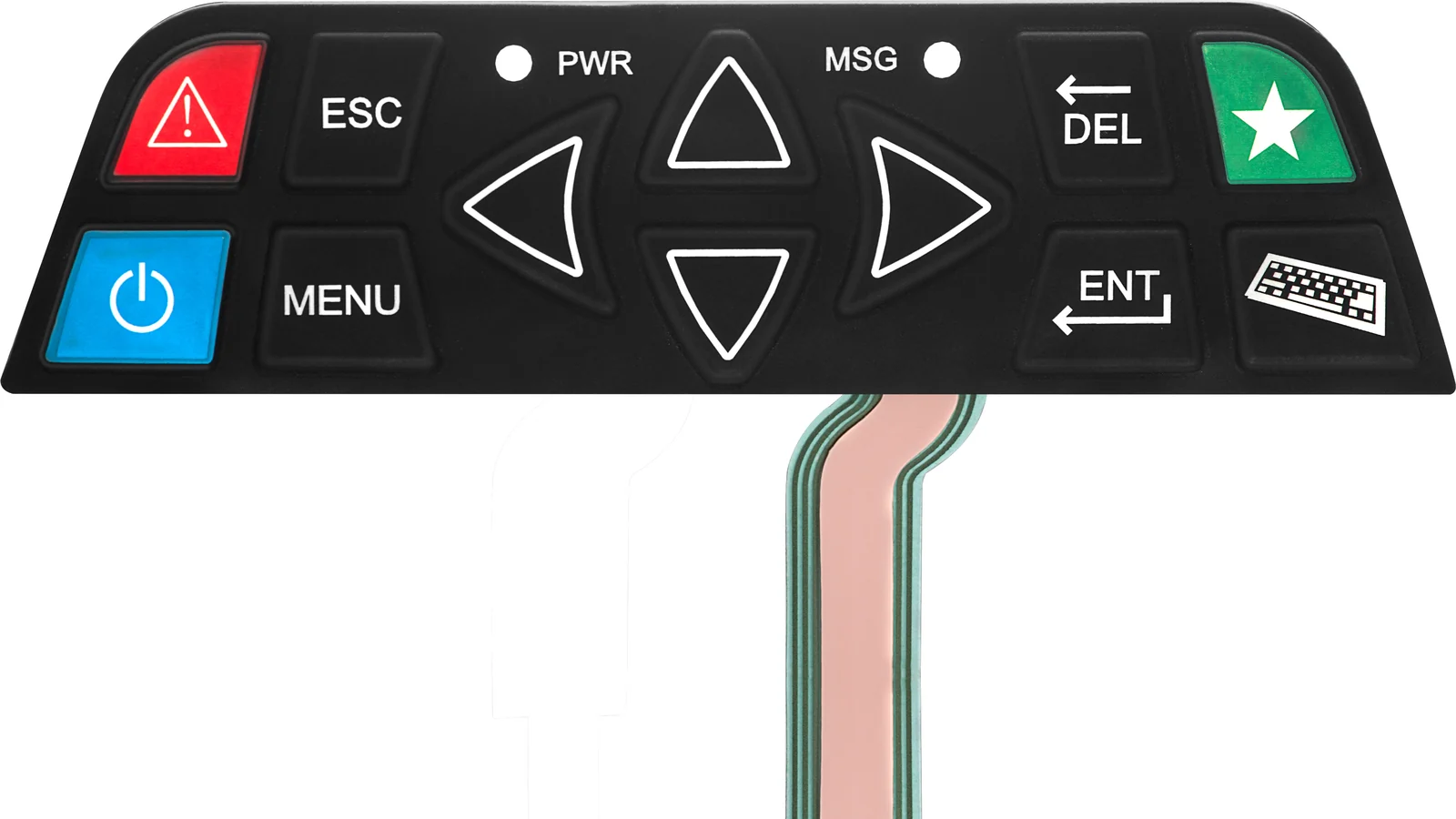
Adding a light source after the overlay artwork is approved is not LED integration. By then, the connector may lack pins, the controller may not have enough voltage headroom, and the spacer may have nowhere to clear the package. A useful design starts with the controller interface and ends with a powered first article in representative hardware.
For buyers evaluating a complete assembly, LED membrane switches combine the printed interface, switch circuit, discrete indicators or illuminated zones, and flexible tail. The supplier still needs project-specific electrical and optical inputs. A color name, a supply label, and a marked circle on the artwork are not enough to release a circuit.
This guide follows the decisions in the order they should be frozen: lighting task, driver, LED bill of materials, branch layout, carrier, pocket, masking, enclosure, and acceptance test. Component values shown below belong to named data sheets; they are examples of evidence, not default values for a new design.
1. Freeze the LED design inputs before routing the circuit
An LED membrane switch needs one controlled interface record shared by the OEM electronics team, overlay designer, circuit designer, and manufacturer. If any row is open, the drawing should remain under review.
| Input to freeze | What the release record must state | What goes wrong when it is missing |
|---|---|---|
| Lighting task | Status point, illuminated legend, key zone, or broad-area backlight | A point source is asked to illuminate an area it cannot cover |
| Controller output | Rail minimum and maximum, source/sink topology, output drop, current limit, and power-up state | A channel is dim, overdriven, or flashes during boot |
| LED identity | Manufacturer, full part number, color/bin rule, approved alternates, polarity mark, and revision | Forward-voltage and optical assumptions change between lots |
| Drive method | Series resistor, constant-current sink, PWM, or multiplexed bank | Resistor ownership and timing remain undefined |
| Circuit carrier | Printed PET, copper FPC, or rigid PCB/hybrid | Trace resistance, attachment process, and local support are guessed |
| Mechanical stack | Package drawing, attachment height, pocket layers, diffuser or guide, overlay, adhesive, and enclosure land | The overlay crowns or a nearby dome loses travel |
| Optical target | Lit and unlit appearance, viewing position, ambient condition, camera method, and approved sample | "Looks bright" changes with each reviewer |
| Production test | Nets powered, test limits, channel combinations, fixture connector, and evidence retained | A panel can pass continuity while an LED remains reversed |
The shortest useful LED definition is therefore not "green indicator." It is closer to: named LED part, driven by a named controller output under stated rail limits, visible through a defined window from a defined viewing condition, with a defined first-article comparison method.
1.1 Separate the lighting circuit from the key matrix
The switch matrix reports contact closure. The LED network consumes current and may switch quickly. They can share one flexible tail, but they should not share undocumented returns, scan timing, or connector pins. The interface table should identify LED anodes, cathodes, common rails, switch rows, switch columns, shields, and reserved pins as different functions.
1.2 Treat the enclosure as part of the optical stack
Internal ribs can shadow a window. A reflective wall can brighten a neighboring legend. A mounting recess can compress the LED pocket. Optical approval on a loose panel proves the panel's appearance only in that fixture; it does not prove the installed appearance. The representative enclosure, bezel, window, and controller state belong in first-article review.
2. Select the lighting architecture by visual job
Discrete indicators, direct-lit legends, light-guide film, and external light pipes solve different problems. The correct choice is the one that meets the visual task with a controllable electrical and mechanical stack.
| Architecture | Best visual job | Circuit consequence | Mechanical and optical consequence | Early decision test |
|---|---|---|---|---|
| Discrete status LED | Power, alarm, communication, or mode point | Dedicated or banked drive nets | Local pocket and small controlled window | Can every status be identified without lighting a neighboring symbol? |
| Direct-lit legend or key | One icon or a small key zone | More channels and higher simultaneous load | Source-to-window distance and diffusion control the hotspot | Is the source hidden from the real viewing position? |
| Side-lit light-guide film | Several legends or a broad zone | Edge-source circuit and shared drive | Guide extraction pattern, reflector, mask, and compression must be reviewed together | Does a powered sample meet corner-to-center uniformity criteria? |
| External light pipe | Remote LED on a host PCB | Membrane may carry no LED power | Housing owns pipe retention, alignment, and leakage control | Can tolerance stack keep the pipe centered over the window? |
| PCB-backed hybrid | Dense sources, local driver, or rigid connector | Host electronics can sit directly behind the interface | Rigid keep-out and housing support replace an all-flex stack | Does the enclosure accept the rigid region and assembly sequence? |
A broad illuminated legend is not automatically a "larger status LED." Enlarging the window can reveal the die, bond wire, or bright center. Conversely, using light-guide film for two isolated alarm points can add tooling and optical development without improving the status task.
The decision also changes the RFQ. A status design needs an explicit net and pocket for each point. A light-guide design needs edge-source location, extraction artwork, reflector, masking, and uniformity criteria. An external pipe shifts several tolerances from the membrane drawing to the enclosure drawing.
3. Choose the circuit carrier and branch topology together
Printed PET, copper FPC, and rigid PCB hybrids cannot be compared by thickness alone. They support different conductor resistance, component attachment, bend behavior, and inspection methods.
| Carrier | Appropriate LED scope | Design record needed | Boundary to verify |
|---|---|---|---|
| Printed PET with silver conductors | Limited status channels where the validated attach process and voltage drop are acceptable | Printed conductor geometry, measured path resistance, attachment material, cure process, and local stiffening | Long shared returns can create unequal voltage at distant LEDs |
| Copper FPC | Tighter routing, lower conductor resistance, soldered SMD parts, or more channels | Copper stack, coverlay openings, bend zones, component land, and assembly drawing | Components and joints must stay out of unsupported dynamic bends |
| Rigid PCB or rigid-flex hybrid | Local driver, dense LED field, retained connector, or mechanical support | Board stack, component keep-outs, fastening, interface connector, and enclosure datums | The rigid region changes housing depth and assembly order |
PCB and FPC membrane switch circuits are relevant when a printed silver circuit cannot meet the electrical or assembly requirement. IPC-2223E describes design requirements for flexible and rigid-flexible printed boards and component mounting forms S3. It does not turn a printed silver PET membrane into an IPC-2223E copper flex, and it does not choose the LED attachment process for the project.
3.1 Use a pin table that can be tested without interpretation
Every LED row should contain:
- connector pin and net name;
- LED reference designator and full part number;
- anode and cathode orientation;
- controller output type;
- current-setting component and its physical owner;
- shared-return or shared-supply group;
- expected power-up state;
- channel combinations used by the end-of-line test.
Polarity must appear on the schematic, footprint, assembly view, and tail pin table. A single symbol on one drawing is not enough when the product passes through CAD export, artwork preparation, placement, lamination, fixture design, and cable assembly.
3.2 Pick the branch pattern from fault behavior, not pin count alone
| Pattern | Advantage | Failure interaction | Suitable release condition |
|---|---|---|---|
| Dedicated pair per LED | Simple diagnosis and no shared-path brightness shift | Connector uses the most pins | Few high-priority indicators with independent acceptance tests |
| Common return with individual drives | Reduces connector pins | Return resistance affects every active branch | All-on voltage drop is calculated and measured at the farthest branch |
| Common supply with individual sinks | Fits open-drain or constant-current sink control | Supply path becomes the shared limit | Driver compliance and common-path drop are included in worst-case analysis |
| Multiplexed rows and columns | Saves pins for a large field | Ghosting, duty cycle, boot state, and firmware timing become system variables | Controller timing and inactive-state behavior are released with the hardware |
An LED matrix should never be inferred from a switch matrix. The two can have different scan rates, diode requirements, inactive states, and fault consequences. If firmware owns multiplexing, the firmware revision and timing assumptions belong in sample approval.
4. Calculate current from the selected LED and controller limits
The resistor value is an output of the electrical model, not a catalog habit. For a simple voltage-driven branch, the useful equation is:
I_LED = (V_RAIL - V_DRIVER - V_F - V_PATH) / R_TOTAL
R_TOTAL includes the current-setting resistor, its tolerance, and any conductor resistance intentionally included in the model. V_PATH includes the supply and return path drops not already represented by resistance. The design should solve at least two corners:
- Maximum-current corner: highest rail, lowest LED forward voltage, lowest driver drop, lowest resistance, and the relevant low-temperature behavior.
- Minimum-light corner: lowest rail, highest LED forward voltage, highest driver and path drop, highest resistance, and the relevant operating temperature.
The controller output limits matter as much as the diode. A GPIO source, low-side transistor, open-drain output, and constant-current sink present different headroom and fault behavior. A constant-current driver such as the TI TLC59108 family can control multiple channels and PWM states, but its compliance range, current setting, power dissipation, and power-up behavior still require a design review S5.
4.1 Why a generic color range is unsafe
Two named Kingbright parts illustrate the problem. Both use a 1.6 x 0.8 x 0.25 mm SMD outline, yet their electrical and ESD data are not interchangeable.
| Data-sheet field | APG1608CGKC-T green | APG1608QBC/D blue | Design implication |
|---|---|---|---|
| Data-sheet revision | V.5B, 2026-01-20 | V.17B, 2025-03-13 | Archive the revision used for calculation |
| Forward voltage at the stated 20 mA characterization condition | 2.1 V typical, 2.6 V maximum | 3.3 V typical, 4.0 V maximum | One resistor calculation cannot represent both colors |
| Luminous intensity at the stated 20 mA condition | 20 mcd minimum, 50 mcd typical | 40 mcd minimum, 100 mcd typical | Brightness acceptance needs the selected part and optical stack |
| Viewing angle, 2theta1/2 | 120 degrees | 130 degrees | Window and viewing position must be evaluated with the selected lens |
| DC forward current listed under absolute maximum ratings | 30 mA | 30 mA | An absolute maximum is not the normal operating target |
| HBM ESD threshold stated by the data sheet | 3000 V | 250 V | Handling controls depend on the exact part, not just package size |
Sources: Kingbright APG1608CGKC-T S1 and APG1608QBC/D S2. Excessive current or temperature causes severe light degradation or premature failure. Their curves are measured under stated fixture conditions. The green sheet, for example, reports thermal resistance on an FR-4 board with a defined pad area; that value cannot be copied into a laminated PET calculation.
4.2 Build the calculation record around min/max evidence
The released calculation should show the rail limits, driver drop limits, LED V_F limits at the intended operating point, resistor tolerance, printed or copper path resistance, simultaneous channel state, and temperature assumption. If the data sheet does not publish a needed corner, the gap should be closed by supplier data or a measured characterization plan, not by inventing a midpoint.
PWM changes average light and average power, but it does not erase peak-current, driver-headroom, or pulse-limit requirements. The controller's duty cycle, frequency, startup state, and diagnostic pulses should be tested on the actual panel because a camera and a human observer can respond differently to flicker.
5. Size the LED pocket from the mechanical drawing
The LED pocket is a controlled cavity, not a clearance circle copied from a package nickname. It has to protect the component and attachment while controlling the light path to the overlay.
For the two Kingbright parts above, the data-sheet body is 0.25 mm thick and the dimensional drawing carries its own tolerance [S1][S2]. The project pocket still needs more inputs:
- maximum component body and terminal geometry from the current drawing;
- solder or conductive-adhesive attachment profile;
- local circuit and stiffener thickness;
- spacer and adhesive thickness after lamination;
- lamination squeeze and die-cut registration capability;
- mechanical clearance needed to avoid preload;
- diffuser, reflector, collar, or guide thickness;
- enclosure support beneath and around the pocket.
The correct cavity height is the result of that stack. A fixed added clearance cannot be declared without the supplier's process capability and the enclosure load path.
5.1 Keep LED cavities out of the key's working geometry
A nearby metal dome needs room to snap, travel, and return. A non-tactile contact needs a vent and spacer opening that do not collapse. The LED cavity must not cut the dome retention land, create a leak path into a switch vent, or leave the overlay unsupported where the operator presses.
This is why the LED map, dome map, vent map, tail route, and adhesive pattern should be reviewed in one stack drawing. Separate artwork files can look valid while their combined cutouts leave a narrow web that shifts during lamination.
5.2 Define the window as an optical system
| Optical element | Controlled variable | Typical defect when uncontrolled | First-article evidence |
|---|---|---|---|
| Translucent icon ink | Transmission, color, and print build | Dim or color-shifted symbol | Approved lit sample under stated drive and ambient light |
| Opaque mask | Coverage and registration | Halo, glowing edge, or visible inactive icon | Unlit and lit photographs from the defined viewing position |
| Diffuser | Material, thickness, surface, and gap | Hot center or excessive light loss | Uniformity image with exposure locked |
| Light-guide film | Source coupling, extraction pattern, reflector, and compression | Bright edge and dark corner | Zone map in representative enclosure |
| Smoked or dead-front window | Unlit concealment and lit transmission | Icon visible when off or unreadable when on | Paired off/on sample with the same camera settings |
| Enclosure cavity | Wall color, ribs, support, and depth | Shadow, reflection, or neighboring-zone leakage | Powered panel installed in representative hardware |
Graphic overlays control more than printed appearance in a lit assembly. Mask density, translucent color, surface texture, embossing, and window registration all change what reaches the operator. Approving only the PDF artwork leaves the optical stack unapproved.

6. Separate thermal, ESD, and assembly evidence
Three different evidence sets are often collapsed into one vague "LED reliability" statement. They should remain separate.
6.1 Component ratings do not describe the laminated assembly
The Kingbright data sheets publish absolute maximum ratings, electrical curves, temperature behavior, solder profiles, and thermal resistance under named conditions [S1][S2]. A membrane assembly changes the board material, copper or printed conductor, pad geometry, adhesive, airflow, and enclosure. The project therefore needs an all-on power state, path-drop measurement, local temperature observation, and post-stress optical check on the production-intent stack.
For always-on banks, calculate both the branch dissipation and the common connector load. For sealed equipment, include the enclosure's internal temperature rather than room ambient. If a rigid PCB island carries a driver, evaluate that island and its attachment as part of the heat path.
6.2 Component handling ESD is not equipment immunity
Kingbright identifies both example LEDs as electrostatic-discharge-sensitive devices and specifies grounded handling precautions [S1][S2]. That governs storage, placement, rework, and assembly benches. The very different HBM thresholds in the two data sheets show why the approved alternate list cannot ignore ESD data.
IEC 61000-4-2:2025 addresses immunity requirements and test methods for electrical and electronic equipment subjected to static-electricity discharges S4. It does not replace component handling controls, and a membrane switch alone does not become "IEC 61000-4-2 certified" because an LED is mounted inside it. The end-product plan must define discharge points, enclosure state, grounding, controller operation, performance criteria, and exact test level.
6.3 Attach the component with a released process
The APG1608 data sheets provide lead-free reflow guidance for the named devices [S1][S2]. That guidance is only one side of the joint. Copper FPC, rigid PCB, conductive adhesive, low-temperature materials, and printed PET each impose different process limits. The assembly drawing should name the attachment material, profile or cure record, placement orientation, allowable rework, cleaning restriction, and inspection method.
7. Match the LED design to the equipment use case
The same LED part can behave differently when the status logic, ambient light, duty cycle, and enclosure change. These five scenarios illustrate which inputs deserve priority.
7.1 Industrial machine panel
Alarm and mode indicators must remain distinct under factory lighting and at the operator's normal angle. The release package should prioritize shared-return drop, simultaneous alarm states, gloves near illuminated keys, enclosure shadows, and a powered inspection fixture that cycles every status combination.
7.2 Medical equipment subassembly
Status colors, brightness states, cleaning exposure, ESD behavior, and risk controls are owned by the device program. The membrane supplier can build and test the component to the approved drawing, but the OEM must connect color meaning, fault response, and equipment qualification to the device's design controls. A component data sheet cannot substitute for that system record.
7.3 Battery-powered handheld controller
Rail sag, sleep current, startup flashes, PWM behavior, and low-battery visibility usually dominate. The minimum-light corner should use the controller's lowest valid rail and actual output drop. A constant-current sink may simplify matching, but its quiescent and compliance requirements still enter the power budget.
7.4 Appliance dead-front interface
The off-state appearance can matter as much as brightness. Opaque backing, translucent icon ink, surface finish, neighboring light leakage, and internal reflections should be approved in the final color and enclosure. The camera settings used for comparison need to be fixed; automatic exposure can make every sample appear acceptable.
7.5 Outdoor or vehicle-mounted control
Daylight contrast, night dimming, temperature, condensation, sealing interfaces, and vibration can interact. The optical requirement should distinguish direct sun, shade, and darkness. Qualification should use exact program methods from the applicable IEC 60068 parts or customer specification, not a blanket reference to the IEC 60068 family S8.
8. Diagnose LED failures by measurement
LED defects become easier to correct when the team records the powered state, location, and measurement instead of describing the sample as "too dim."
| Observed symptom | Likely variables | First measurements | Drawing or process owner |
|---|---|---|---|
| One channel never lights | Polarity, open joint, wrong pin, damaged LED, disabled driver | Pin-to-pin continuity, diode test, controlled-current illumination, controller state | Schematic, placement, fixture, firmware |
| One color is much dimmer | Incorrect V_F model, wrong resistor, bin mix, window transmission | Branch voltage/current, part marking, resistor value, lit window comparison | BOM, circuit, overlay |
| Farthest LEDs dim when all are on | Shared path or connector drop | Voltage at near and far branches in single-on and all-on states | Trace geometry, connector, harness |
| Neighboring symbol glows | Mask opening, cavity leakage, reflector, enclosure reflection | One-channel-at-a-time dark-room image and physical alignment | Overlay, spacer, enclosure |
| Bright crescent or dark edge | Source-to-window registration, pocket, diffuser gap | Overlay/circuit datum measurement and locked-exposure image | Die cutting, printing, lamination |
| Nearby key feels different | Pocket preload, cutout overlap, local support loss | Stack section, flatness, force-displacement comparison | Spacer, adhesive, enclosure |
| Intermittent after flexing | Component in bend, unsupported joint, cracked conductor | Bend-zone review, microscope inspection, resistance during controlled motion | FPC layout, stiffener, assembly |
| Works at room temperature only | Rail headroom, V_F shift, driver drop, joint or adhesive stress | Powered temperature profile using project limits | Electronics, BOM, qualification plan |
The testing and quality plan should connect each acceptance result to the released BOM, drawing revision, fixture revision, power conditions, and sample identity. A photograph without those fields documents appearance, but not repeatable evidence.
9. Move from RFQ to approved first article in seven gates
An efficient LED project does not begin by asking the manufacturer to choose a random source. It begins with a small evidence package and closes each open variable before volume tooling.
- Lighting brief: mark every status point, legend, and zone in lit and unlit artwork.
- Controller interface: release rail limits, drive topology, output-drop limits, startup state, PWM or multiplex timing, and simultaneous-on combinations.
- LED BOM: select full part numbers, approved alternates, color/bin rules, data-sheet revisions, and handling class.
- Circuit release: approve schematic, net names, polarity, resistor or driver ownership, carrier, connector, and measured path-resistance plan.
- Stack release: approve package section, attachment, pocket, dome/vent separation, diffuser or guide, masks, adhesive, and enclosure support.
- Electrical first article: test open, short, polarity, branch current, all-on drop, inactive-channel leakage, and controller states.
- Optical and haptic first article: view the installed panel under agreed conditions, compare lit and unlit states, and verify nearby key response before the approved sample is sealed.
Prototype validation is most useful when each sample answers a named question. If the first build changes the LED part, mask, pocket, resistor, and enclosure at once, the team cannot identify which change corrected or created the defect.
RFQ attachment checklist
- LED schematic or net table with polarity;
- controller output data and rail limits;
- selected LED data sheets and approved alternates;
- overlay artwork with separate translucent and opaque layers;
- cross-section and enclosure drawing near each light source;
- status truth table or PWM/multiplex timing;
- powered inspection states and viewing condition;
- environmental and equipment-level test requirements;
- first-article evidence format and approval owner.
10. Frequently Asked Questions
What is LED membrane switch circuit design?
LED membrane switch circuit design is the coordinated electrical, mechanical, and optical plan for driving LEDs inside or behind a laminated interface. It defines the controller, LED part number, polarity, current setting, carrier, pocket, window, enclosure, and production tests. Overlay artwork alone does not define the circuit.
How should membrane switch LED wiring be documented?
Document each LED with a reference designator, full part number, anode, cathode, connector pin, net name, drive type, current-setting component, shared rail, and test state. Use the same polarity convention on the schematic, footprint, assembly view, and tail table so placement and fixture teams do not reinterpret it.
What resistor value should an LED membrane switch use?
There is no universal resistor value. Calculate the branch from maximum and minimum rail voltage, driver drop, selected LED forward-voltage limits, path resistance, resistor tolerance, temperature, and required current. Then measure the production-intent branch. A value copied from another color or controller can overdrive one LED and starve another.
Can LED lines share a flexible tail with the switch matrix?
Yes. LED and key-matrix nets can use the same tail and connector when every pin, return path, current, and inactive state is defined. Keep LED load current from changing key-sense references, and verify all-on, boot, PWM, and multiplex states on the actual controller.
When should copper FPC replace a printed PET LED circuit?
Copper FPC becomes the stronger candidate when path resistance, routing density, soldered component attachment, bend control, or channel count exceeds the validated printed PET process. The decision should come from measured drop, assembly capability, and mechanical constraints, not from a blanket claim that one carrier is always better.
How is LED pocket height determined?
LED pocket height comes from the maximum component drawing, attachment profile, circuit and stiffener thickness, spacer and adhesive after lamination, process tolerances, optical layers, and enclosure load. The package nickname does not supply those values. Confirm the calculation with a sectioned or measured production-intent sample.
Why can a correct LED circuit still show a hotspot?
A hotspot is usually an optical-path problem rather than an open circuit. Source position, lens angle, window size, diffuser gap, mask registration, light-guide extraction, and enclosure reflections determine what the operator sees. Review powered samples with fixed drive, ambient light, camera exposure, distance, and angle.
Does IEC 61000-4-2 qualify an LED membrane switch?
No. IEC 61000-4-2:2025 defines equipment immunity test requirements and methods for electrostatic discharge. Component handling ESD, membrane assembly checks, and finished-equipment immunity are separate controls. The device program must define the enclosure, discharge points, operating state, test level, and performance criteria.
What should be approved on the first LED membrane switch sample?
Approve part identity, polarity, branch current, all-on voltage drop, inactive-channel behavior, connector mapping, overlay flatness, nearby key feel, lit and unlit appearance, viewing conditions, and installation in representative hardware. Record the drawing, BOM, controller, fixture, and sample revisions with the signed result.
Technical Sources
Technical values are tied to the named document, product grade, and stated test boundary.
| ID | Primary source | Scope used in this article |
|---|---|---|
| S1 | Kingbright, APG1608CGKC-T data sheet, Rev. V.5B, 2026-01-20 | Green LED dimensions, electrical/optical conditions, ratings, ESD and reflow notes |
| S2 | Kingbright, APG1608QBC/D data sheet, Rev. V.17B, 2025-03-13 | Blue LED dimensions, electrical/optical conditions, ratings, ESD and reflow notes |
| S3 | IPC, IPC-2223E table of contents and scope | Flexible and rigid-flexible printed-board design scope |
| S4 | IEC, IEC 61000-4-2:2025 official record | Finished-equipment electrostatic-discharge immunity scope |
| S5 | Texas Instruments, TLC59108 data sheet | Example of an I2C-controlled constant-current LED sink and PWM architecture |
| S6 | Texas Instruments, LED-driver product group | Driver topology and data-sheet selection context |
| S7 | IPC, board design standards overview | Relationship between generic, rigid, and flexible board design standards |
| S8 | IEC, IEC 60068-1 official record | Environmental testing framework and need to select exact methods and severities |
| S9 | IEC, basic EMC publications | IEC 61000-4 series context |
| S10 | Kingbright, application notes index | Component handling and application-note reference point |
Freeze the controller-to-window chain before tooling
Send the controller limits, selected LED data sheets, pin table, stack section, lit and unlit artwork, enclosure detail, and first-article criteria. JASPER Engineering will identify open electrical, pocket, masking, and evidence decisions before release.