
Plan wearable biosensor electrode patch design in 8 decisions: skin interface, printed electrodes, interconnects, encapsulation, testing, and packaging.
1. Start with the system boundary, not a favorite material
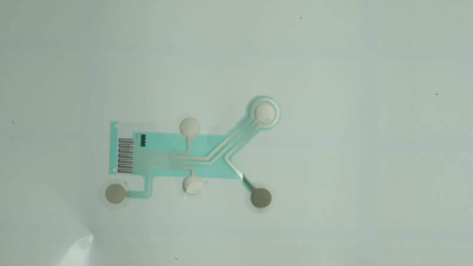
A wearable biosensor patch is a body-worn layered assembly that places one or more sensing elements at a defined location, routes their output through flexible conductors, and connects them to local or remote electronics. A printed electrode is one part of that system. It may be exposed to skin, coupled through a hydrogel, functionalized for an electrochemical target, or insulated for capacitive measurement. Those choices are not interchangeable.
The strongest first input is a one-sentence sensing objective: measure X at body site Y for use condition Z. 2M Engineering and TNO@Holst identify the measured physiological parameter, body location, target population, setting, wear duration, and monitoring-versus-intervention objective as configuration drivers. That list should reach the electrode converter before artwork begins (2M Engineering/TNO@Holst, 2021).
For a program that needs a converted wearable biosensor patch, the request should define the boundary of supply. Does the converter deliver printed electrodes on film, a die-cut adhesive/electrode laminate, a flex tail with connector contacts, or an assembled patch that accepts an electronics module? The answer changes material control, inspection points, traceability, packaging, and who owns each verification activity.
Three distinctions prevent early confusion:
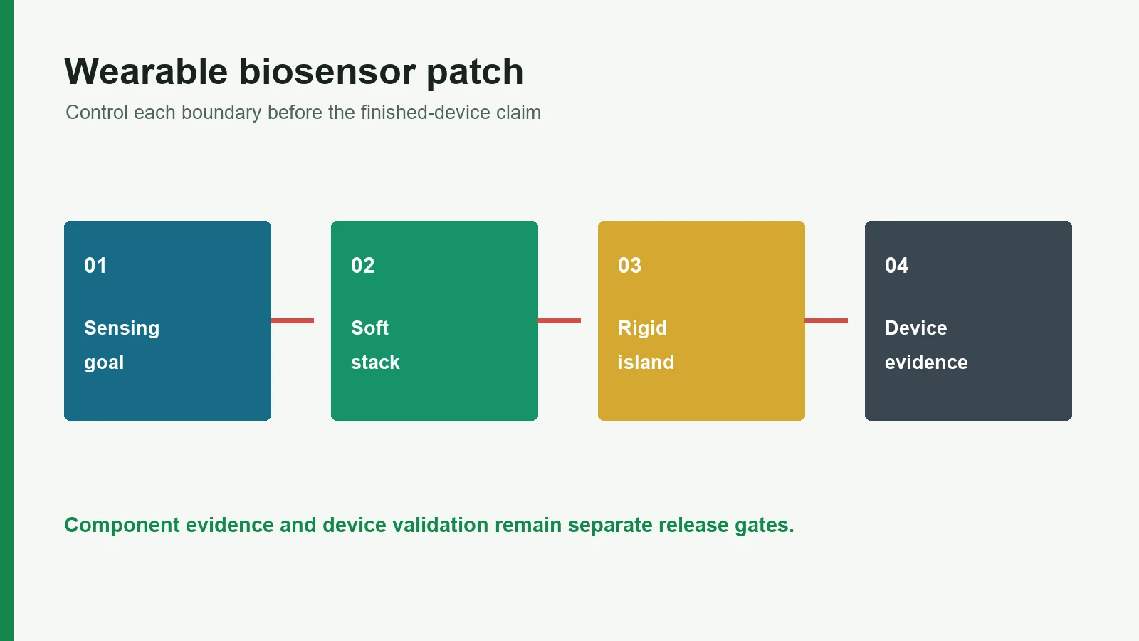
- Component fabrication is not finished-device validation. Printed traces, die-cut layers, and converted subassemblies can be inspected against drawings. They do not establish clinical accuracy, usability, biological safety, or regulatory status.
- Material documentation is not device evidence. A supplier datasheet can narrow candidates. It cannot prove that a specific ink, adhesive, hydrogel, film, and process sequence is suitable in the final contact scenario.
- A low-profile coupon is not a worn patch. The body site adds curvature, sweat, hair, motion, application variation, and removal forces that a flat bench coupon does not reproduce.
Lim and co-authors group wearable skin-electrode requirements into mechanical, electrical, and biological considerations. Their 2024 review links flexibility, adhesion, conformability, electrode–skin impedance, signal-to-noise ratio, and breathability rather than treating them as isolated properties (Communications Materials, 2024). That coupling is the reason the stack must be decided as a system.
2. Reference stack for a printed medical sensor patch
A printed medical sensor patch can contain fewer layers than the reference below, or several sublayers inside each block. The order is a design map, not a universal recipe.
OUTSIDE / ENVIRONMENT
8 Outer cover, label, or breathable protective film
7 Encapsulation / edge seal around vulnerable features
6 Rigid or semi- · Battery, AFE, MCU, radio, antenna,
rigid island · connector, or removable module
5 Interconnect transition / reinforcement / strain path
4 Printed dielectric, coverlay, or selective insulation
3 Printed conductors, electrode sites, and contact pads
2 Flexible substrate: film, elastomer, or hybrid carrier
1 Skin interface: adhesive zone, gel, dry contact,
spacer, vent pattern, or insulated sensing window
0 Release liner with split, tab, and application logic
SKIN / MEASUREMENT INTERFACE
Diagram description: Cross-section of a skin wearable electrode patch. A release liner covers the skin-contact layer. Above it sit the flexible substrate, printed electrode and conductor pattern, selective dielectric, interconnect transition, rigid electronics island, encapsulation, and outer protective layer. Functional electrode windows remain open where the sensing principle requires contact.
Molex presents a disposable patch architecture that includes BLE, a printed antenna, a thin-film battery, a flexible substrate, hydrogel and electrodes, adhesive, and a release liner. Its related article contrasts electronics mounted directly on a disposable PET substrate with a reusable “puck” connected to a disposable electrode portion. Texas Instruments’ medical-patch block diagrams add another view: ECG electrodes, an analog front end, ESD/defibrillation protection, power management, processing, memory, and wireless communication can all affect the interface presented to the flexible layer (Molex disposable patches; Molex architecture article; Texas Instruments).
The layer sequence must therefore be read in both directions. From skin upward, it controls contact, movement, and moisture. From electronics downward, it controls signal routing, power, shielding, strain transfer, and assembly temperature. The transition between the soft field and the rigid island often carries more integration risk than either area alone.
Layer decision table
| Layer / function | Candidate family—not a specification | Drawing input that matters | Common integration risk |
|---|---|---|---|
| Skin securement | Acrylic or silicone pressure-sensitive adhesive; hydrocolloid-based system; patterned adhesive | Contact footprint, wear scenario, removal direction, venting, no-adhesive zones | Edge lift, skin loading, adhesive creep into an electrode window |
| Electrode interface | Dry metal/carbon contact; Ag/AgCl with electrolyte or hydrogel; functionalized electrochemical surface; insulated capacitive electrode | Exposed area, spacing, reference/counter/working roles, surface finish, contamination limit | Interface impedance drift, dehydration, shorting, inconsistent contact area |
| Flexible carrier | PET, polyimide, TPU/elastomer, nonwoven-supported laminate, hybrid flex | Thickness, grain/direction, bend axis, stretch field, die-cut geometry | Buckling, crack initiation, modulus mismatch, dimensional change during cure |
| Printed conductor | Silver, silver/silver-chloride system, carbon, conductive polymer, or hybrid stack | Trace width/space, dry thickness, cure limit, resistance method, contact finish | Cure incompatibility, migration/corrosion, abrasion, resistance change under strain |
| Dielectric / cover | Printed dielectric, coverlay film, selective encapsulant | Openings, overlap, registration tolerance, edge distance, cure sequence | Pinholes, blocked electrode, fluid path, stress concentration at termination |
| Electronics transition | Printed tail, FPCB, anisotropic interconnect, crimp/contact pad, snap, connector, removable puck | Datum, pitch, plating/contact surface, reinforcement, insertion/removal load | Pad peel, fretting, rigid-edge cracking, assembly misregistration |
| Protection | Conformal encapsulant, overmold, barrier film, top tape, edge seal | Keep-outs, vent paths, exposed sensor surfaces, rework boundary | Trapped moisture, stiffness step, antenna detuning, incomplete seal |
| Release and pack | Coated paper/film liner, split liner, pouch, tray, carrier card | Split location, pull tab, peel direction, orientation, label and lot scheme | Electrode contamination, adhesive transfer, pre-release, application damage |
Solventum’s wearable framework separates skin-contact, device-assembly, and outer-protective layers. Avery Dennison Medical lists acrylic, silicone, and hydrocolloid adhesive families ; substrate, moisture, movement, wear duration, and intended population affect selection (Solventum; Avery Dennison Medical). These are useful candidate categories. They are not proof that a material is safe or effective in a finished device.
3. The 8 decisions in wearable biosensor electrode patch design
The eight decisions below should appear in the design input record, drawing package, or verification plan. Each closes one class of ambiguity before tooling or production material is committed.
3.1 Define intended use, sensing objective, and operating conditions
Start with the measurand and transduction method. A biopotential electrode, resistive temperature element, electrochemical sweat sensor, and capacitive electrode impose different requirements on exposed area, reference geometry, moisture access, dielectric coverage, and electronics input. Body location also matters: the forearm, chest, abdomen, and joint regions present different curvature and motion paths.
Record at least: body site, application method, expected motion, contact duration, temperature/humidity exposure, sweat or water exposure, single-use versus reusable elements, powered versus passive operation, signal amplitude/frequency band, and interface to the analog front end. If the patch supports a medical-device claim, the legal manufacturer must also define intended users, use environment, and relevant risk controls.
For a 16-day planning input, the prototype plan should at least condition the production-intent stack through the full intended interval and define interim checks appropriate to the risk: edge lift, electrode contact or interface impedance, conductor continuity, interconnect integrity, user/application observations, and post-removal inspection. Those checks are planning categories. Their methods, sample size, body site, population, and acceptance criteria still belong to the device owner’s risk and verification plan.
the drawing request names the sensing objective, body site, interface type, wear scenario, and supply boundary in one revision-controlled document.
the requirement says only “medical-grade wearable electrode” or asks the converter to choose a standard stack without a defined use condition.
3.2 Choose the skin interface before choosing the adhesive
The skin-contact layer has two jobs that can conflict: maintain the patch position and maintain the intended electrical or chemical interface. A hydrogel/electrolyte path, dry electrode, micromachined surface, and insulated capacitive electrode solve different problems. The securement adhesive may surround the electrode, sit on a separate carrier, or form a patterned field; it should not be allowed to flow into a functional window by accident.
Poor adhesion reduces electrode contact area, while poor conformability creates voids and can disrupt consistent acquisition. The same review explains that electrode–skin impedance depends on contact area and interface conductivity; wet and semi-dry electrodes can show lower impedance than dry electrodes under the reviewed conditions (Lim et al., 2024). That is a conditional design relationship, not a rule that every gel electrode is preferable.
the electrode-contact zone, securement zone, vent/opening pattern, edge margin, and removal direction are separately dimensioned.
peel strength to stainless steel is used as the only criterion for a skin wearable electrode patch.
3.3 Match substrate mechanics to the body and the rigid island
“Flexible” says little by itself. PET and polyimide films bend, but a complete laminate may not stretch enough for a high-strain body location. An elastomer can stretch, yet printed traces, dielectric, component joints, and an adhesive laminated to it may become the limiting elements. The design should identify where bending is allowed, where in-plane strain is expected, and where a rigid or semi-rigid island interrupts the field.
A useful mechanical drawing marks the neutral-axis intent, minimum bend region, strain-relief geometry, rigid-component keep-out, tail direction, and die-cut radii. Serpentine traces can redistribute strain, but geometry must be evaluated with the actual conductor/dielectric/substrate stack. The Phan et al. Prototype used a double-layer FPCB and mounted components; its architecture demonstrates integration, not a transferable mechanical limit (Biosensors, 2022).
the team supplies a body-envelope or fixture, motion direction, bend/strain map, and rigid-island boundary before conductor artwork is frozen.
a flex coupon passes flat continuity testing, so the assembled laminate is assumed to survive application, wear, and removal.
3.4 Specify the flexible biosensor electrode, conductor, and dielectric as one system
Conductive ink cannot be selected on sheet resistance alone. The substrate must tolerate the print and cure sequence; the conductor must survive the intended deformation and environment; the dielectric must adhere to both conductor and carrier; and every printed pass must fit the registration budget. Electrode chemistry may impose an additional surface treatment or functional layer that cannot be covered or contaminated.
The drawing should state conductor geometry, allowed resistance and measurement method, electrode area, contact-pad finish, dielectric openings, dielectric-to-conductor overlap, registration tolerance, cure/thermal restrictions, and critical cosmetic or contamination limits. For a custom printed electrode array, channel numbering, electrode role, spacing datum, and tail pinout should be explicit rather than inferred from artwork.
Use witness coupons when they answer a defined question: print thickness, resistance after cure, adhesion to the carrier, registration, or process drift. A coupon cannot replace tests on converted geometry, because die cutting, lamination, bending, and terminal assembly occur later.
ink, substrate, dielectric, print sequence, test coupon, and converted-part acceptance checks form one controlled process plan.
a different conductor or cure cycle is treated as a drop-in substitution because initial resistance is similar.
3.5 Design the interconnect and electronics island around force transfer
The printed electrode ends at an analog front end, connector, FPCB, snap, conductive adhesive joint, crimp, or removable module. That transition changes stiffness and concentrates load. It may also introduce contact resistance, galvanic compatibility questions, assembly pressure, heat, cleaning restrictions, and a new moisture path.
Texas Instruments’ multiparameter patch diagram shows why the boundary matters: ECG electrodes may feed an AFE alongside ESD/defibrillation protection, power management, processing, memory, and radio functions. The flexible converter needs the electrical interface limits and mechanical envelope even when another supplier assembles the electronics (Texas Instruments).
Place strain relief before the rigid edge, keep the joint away from the primary bend line, and define which layer carries peel/removal load. For a reusable puck, specify the mating cycle, alignment feature, contact-wipe behavior, cleaning boundary, and disposable/reusable separation. For a fully disposable island, check that component attachment and encapsulation processes do not damage the skin-side laminate.
the drawing controls datum, contact finish, reinforcement, bend keep-out, pull direction, and electrical test points at the transition.
the tail, connector, or rigid island is added after electrode approval without repeating mechanical and electrical verification.
3.6 Draw encapsulation, exposed windows, vents, and edges explicitly
Encapsulation protects electronics and conductors, but more coverage is not automatically better. An electrochemical sensor may need analyte access. A skin electrode may need ionic contact. An optical path, pressure port, antenna, temperature element, or humidity-responsive layer may need a specific window or material above it. An impervious top film can also change moisture accumulation below the patch.
The DuPont Liveo/STMicroelectronics prototype places skin adhesive/conductive tape, sensors, flexible electronics, and encapsulation in one concept platform (DuPont Liveo prototype sheet). Molex likewise lists custom encapsulation among disposable-patch integration steps. Neither source establishes a universal seal design.
Control the encapsulation boundary with dimensions. Mark functional windows, coating overlap, edge-seal width, vent path, antenna keep-out, connector area, and permissible rework. Avoid abrupt thickness steps over a recurring bend line. Inspect pinholes and coverage using a method tied to the actual failure risk rather than relying on appearance alone.
every exposed and covered surface has a reason, a drawing boundary, and an inspection method.
“encapsulate all electronics” is the complete requirement, with no window, edge, or stiffness definition.
3.7 Treat the liner, packaging, storage, and application sequence as design layers
A release liner controls adhesive protection, die-cut stability, converting, presentation, and application. Its split and tab determine where a user grips the patch and whether they touch an electrode or hydrogel. Liner release that is too high can stretch a thin patch during application; release that is too low can cause pre-release during shipping or feeding. These risks cannot be inferred from the adhesive’s steel-panel peel value.
ASTM D3330/D3330M-04(2025) includes methods for pressure-sensitive tape peel and a method for liner-release force. Peel results may not provide design information because no direct relationship necessarily exists between peel adhesion and a functional requirement (ASTM International). Use the standard as a controlled comparison method when applicable—not as proof of on-body wear.
The packaging plan should define orientation, pouch or tray support, barrier need, light sensitivity, humidity control, lot/expiry labeling, shipping conditioning, and the state in which electrical release tests are repeated. Sterile-barrier or shelf-life claims require a separate finished-device packaging program; a converter cannot infer them from film data.
the first article includes the production-intent liner, tab, pouch/tray concept, application sequence, and conditioned testing.
the electrical laminate is approved on a temporary liner, while packaging and application mechanics are deferred until launch.
3.8 Assign verification by sample state and responsible party
A useful test plan separates five levels: material/coupon, printed web, converted patch, assembled electrical device, and finished device in its intended contact and packaging configuration. Each level answers different questions. Conductor resistance on a coupon says nothing about skin contact; peel from steel says nothing about signal artifact during motion; a converted subassembly inspection says nothing about biological response.
FDA’s September 2023 guidance on ISO 10993-1 describes a risk-based biological evaluation for devices with direct or indirect body contact, including intact-skin considerations. It supports a central boundary: supplier labels such as “medical grade” do not replace evaluation of the device’s materials, processing, contact type, and duration (U.S. FDA, 2023).
If the assembled product is medical electrical equipment within scope, IEC 60601-1-2:2014+A1:2020 addresses electromagnetic disturbances and emissions affecting basic safety and essential performance (IEC). Printed-electrode manufacture does not confer IEC 60601-1-2 compliance; the finished-device program must define applicability, essential performance, configurations, and test evidence.
every test row names the sample state, conditioning, method, acceptance criterion, data owner, and change that triggers retest.
a material certificate, supplier brochure, or component test report is presented as finished-device verification.
4. When a printed integrated patch is not the best choice
A thin, integrated patch is attractive when the electrode geometry and flexible routing need repeatable production. It is not automatically the lowest-risk architecture. Choose the construction that isolates the hardest requirement rather than forcing every function into one disposable laminate.
| Project condition | Architecture to consider | Why it may be better than a fully integrated printed patch | New question it creates |
|---|---|---|---|
| Expensive electronics must be reused | Disposable electrode/adhesive carrier plus removable puck | Separates skin-contact consumable from radio, processor, and battery | Contact repeatability, cleaning, mating cycles, user alignment |
| A standard electrode already meets the sensing need | Conventional disposable electrode linked to a separate monitor | Reduces custom electrode and biological-evaluation variables | Cable motion, connector management, user comfort |
| Little body conformity is required and enclosure protection dominates | Rigid or semi-rigid sensor module with separate securement | Simplifies component assembly and shielding | Edge pressure, weight, adhesive loading, motion artifact |
| The sensor needs open fluid access or microfluidics | Hybrid patch with dedicated fluidic/sensing cartridge | Keeps fluid path and printed routing as controlled subassemblies | Sample transport, contamination, evaporation, calibration |
| The body location has high multi-axis strain | Segmented islands, textile architecture, or remote electronics | Avoids forcing brittle conductors and joints through a high-strain field | Inter-island connections, washability, repeatability |
| Very short supervised measurement | Repositionable fixture, strap, or conventional lead system | A long-wear adhesive stack may add cost and validation work without benefit | Placement repeatability and operator procedure |
Molex publicly describes both disposable-electronics and removable-puck layouts. That is a useful architecture fork, not an endorsement of either option for a specific program. The best choice depends on device economics, data continuity, waste strategy, user steps, and the verification burden assigned to each interface.
5. A six-step development process from sensing objective to approved sample
Step 1 — Freeze the input sheet
Create a one-page input sheet before requesting artwork. Include the sensing objective, electrode type, body site, contact duration, motion/moisture scenario, expected users, disposable/reusable split, electronics interface, application method, and boundary of supplier responsibility. Add drawings or photographs only as context; do not let a reference product silently become the specification.
Step 2 — Build a functional stack, then name materials
List every function from skin contact to outer protection. Decide which surfaces must adhere, conduct, insulate, vent, seal, slide, release, or remain exposed. Only then shortlist material families. This sequence prevents a favored adhesive or film from dictating an unsuitable architecture.
Step 3 — Allocate geometry and tolerances
Create one controlled stack drawing and linked artwork files. Dimension electrode areas, gaps, dielectric openings, adhesive windows, edge margins, tail contacts, reinforcement, rigid-island keep-outs, liner splits, and assembly datums. The tolerance study should include print registration, lamination, die cutting, substrate dimensional change, and mating-part position—not just CAD nominal dimensions.
Step 4 — Prototype the risk, not only the appearance
Use coupons for print/cure questions and converted prototypes for stack questions. If electrode-window contamination is the leading risk, inspect that interface. If strain at the electronics transition is the leading risk, bend and pull the actual transition. If application damages the patch, test the production-intent liner and tab. A photogenic flat sample does not close these risks.
Step 5 — Approve samples against a matrix
The first-article package should contain the drawing revision, bill of materials or controlled material references, key process records, inspection data, electrical results, images of critical registration/coverage features, deviation list, and lot identity. Acceptance criteria must be agreed before samples are measured.
Step 6 — Lock change control and finished-device handoff
Define which changes require notification or requalification: substrate, ink, dielectric, adhesive, liner, cure profile, print screen/artwork, die, converting site, electronics attachment, encapsulant, or packaging. Transfer the approved component evidence into the legal manufacturer’s device history and risk-management process. The handoff should make gaps visible rather than implying that component approval closes device validation.
Drawing checklist
- [ ] Sensing objective, body site, environment, and contact duration
- [ ] Electrode function, numbering, exposed area, spacing, and reference datum
- [ ] Substrate material reference, thickness, orientation, and bend/strain zones
- [ ] Conductor geometry, resistance method, contact finish, and test points
- [ ] Dielectric openings, overlap, registration tolerance, and cure restrictions
- [ ] Adhesive footprint, no-adhesive zones, vent pattern, and removal direction
- [ ] Tail/interconnect pitch, reinforcement, rigid keep-out, and mating envelope
- [ ] Encapsulation boundaries, sensor/antenna windows, edge seals, and vents
- [ ] Liner material, split, tab, peel direction, and application sequence
- [ ] Lot marking, packaging orientation, conditioning, and change-control triggers
Sample-approval checklist
- [ ] Materials and process route match the submitted build record
- [ ] Electrode and dielectric registration meet drawing tolerances
- [ ] Functional surfaces are free from adhesive, ink smear, and handling contamination
- [ ] Resistance/continuity is tested before and after the agreed conversion stress
- [ ] Interconnect and reinforcement survive the defined pull/bend sequence
- [ ] Liner removes without stretching, pre-releasing, or contaminating the patch
- [ ] Production-intent application method is demonstrated on the intended fixture or body surrogate
- [ ] Deviations and open device-level tests are listed, not buried in approval notes
6. Failure chains and a responsibility-based test matrix
A patch failure rarely belongs to one material. The initiating condition changes geometry or chemistry; that physical change then alters the electrical interface or assembly. Review the chain, not only the final symptom.
Decision boundaries that must stay visible
| Boundary | Controlled on the component drawing | Requires assembled- or finished-device evidence |
|---|---|---|
| Electrical geometry | Electrode area, trace width/space, contact pad, pinout, and inspection datum | Signal quality, artifact rejection, diagnostic/monitoring performance, AFE interaction |
| Mechanical construction | Layer thickness, die cut, reinforcement, bend keep-out, and transition geometry | Body-site wear, application variability, motion response, removal behavior |
| Material identity | Supplier grade, lot trace, print/cure route, adhesive and liner references | Biological evaluation for actual processing, contact type, duration, and population |
| Adhesive characterization | Converted footprint, liner release, controlled peel/shear methods when applicable | Claimed wear duration, skin response, repositioning, shower/exercise performance |
| Protective architecture | Encapsulation area, overlap, openings, vents, and visual/coverage inspection | Ingress, cleaning, EMC interaction, antenna performance, shelf-life protection |
| Packaging handoff | Part orientation, pouch/tray drawing, label data, and pack-out inspection | Distribution, aging, sterile barrier if applicable, post-storage device function |
Common failure chains
| Initiating condition | Physical change in the stack | Likely consequence | Check that can expose it early |
|---|---|---|---|
| Sweat reaches an unprotected trace edge | Ionic contamination, swelling, or corrosion path | Resistance drift, leakage, intermittent channel | Conditioned converted-part inspection plus electrical test under defined exposure |
| Adhesive edge lifts during motion | Electrode contact area and pressure change | Interface-impedance variation or motion artifact | Application/wear simulation with signal or impedance monitoring defined by device team |
| Rigid island crosses a repeated bend | Strain concentrates at pad or conductor termination | Trace crack, pad peel, intermittent interconnect | Bend test on assembled transition, not bare film only |
| Dielectric registration shifts | Electrode area is partly covered or adjacent conductors lose spacing | Sensitivity change, short/leakage risk, channel variation | Optical registration measurement tied to drawing datums |
| Liner release is too high | Thin laminate stretches during peel/application | Electrode spacing shifts; trace or joint damage | Production-liner application study plus post-application continuity/geometry check |
| Encapsulant creates a sharp stiffness step | Neutral axis and local curvature change | Crack initiation at encapsulation boundary | Cross-section review and repeated bending across the real thickness transition |
| Hydrogel or functional surface loses moisture | Interface chemistry/contact changes | Impedance or sensor-response drift | Packaging/storage conditioning followed by device-specific functional test |
| Assembly heat exceeds a layer’s process window | Film distortion, adhesive change, ink/dielectric damage | Registration loss, delamination, resistance shift | Thermal-history record plus before/after dimensional and electrical checks |
Verification matrix
| Level | Example questions | Suitable evidence | Owner boundary |
|---|---|---|---|
| Incoming material / print coupon | Did the ink cure? Is thickness/resistance within the agreed process window? Does dielectric adhere to the carrier? | Supplier documentation plus lot checks and controlled coupon tests | Material supplier and converter, as contracted |
| Printed web / sheet | Are registration, print coverage, line geometry, and electrical networks stable across the process? | In-process optical and electrical data; statistical plan where defined | Converter |
| Converted patch subassembly | Did lamination, die cutting, liner application, and interconnect assembly preserve function? | Drawing inspection, continuity/resistance, pull/bend, liner/application checks | Converter/integrator per supply boundary |
| Assembled powered device | Do AFE, ESD protection, power, radio, antenna, firmware, and electrodes work together under defined disturbances? | System verification, EMC/safety work where applicable, risk-control tests | Legal manufacturer / device integrator |
| Skin-contact finished device | Is the biological evaluation adequate for materials, processing, contact type, duration, and population? | ISO 10993-1 risk-based evaluation and any justified testing; usability/wear evidence | Legal manufacturer with qualified laboratories/experts |
| Packaged product over claimed life | Does packaging protect the product and preserve application/function through storage and distribution? | Package, transport, aging, seal/barrier, and post-conditioning functional evidence as applicable | Legal manufacturer / packaging owner |
For adhesive characterization, ASTM D3330 can support a controlled peel comparison when its scope fits. It should sit beside—not replace—application, wear, removal, and device-function checks. For biological evaluation, the FDA’s 2023 ISO 10993-1 guidance is a regulatory reference for United States submissions, not a certificate a component vendor can attach to the whole device. For powered medical electrical equipment, IEC 60601-1-2 applies at system level when the product falls within scope.
JASPER’s testing and quality capability page can be used during a project to map available component checks against this matrix. Any test not verified on that page before release should remain a requested capability, not a claimed one.
7. Project input checklist for an electrode-patch review
Send a compact evidence package, even if some fields are still open. It lets the manufacturing team identify the real unknowns instead of quoting an assumed construction.
- Sensing objective: measurand, electrode principle, channel count, frequency/sampling needs, and expected signal path.
- Use envelope: body site, wear duration, motion, sweat/water exposure, temperature, application setting, and removal method.
- Stack concept: exploded view with known films, adhesive zones, gels or functional layers, dielectric, rigid island, encapsulation, and liner.
- Mechanical data: overall dimensions, thickness budget, bend/strain areas, tail route, connector/module envelope, and application fixture.
- Electrical data: electrode geometry, trace requirements, resistance method, pinout, AFE interface, shielding/guarding concept, and test points.
- Manufacturing boundary: parts supplied by each party, assembly sequence, cleanliness controls, packaging state, lot size assumptions, and change-control expectations.
- Verification plan: sample state, conditioning, method, acceptance criterion, owner, and unresolved finished-device work.
Electrode-pad manufacturing and material-selection resources help separate material-family questions from stack-integration questions.
Evidence Release Matrix
| Evidence level | Controlled article | Decision |
|---|---|---|
| Material | Named grade, supplier, lot, process, and conditioning | Candidate input remains within its documented scope |
| Printed component | Released drawing, stack, geometry, connector, and inspection method | The manufactured part matches its component specification |
| Integrated assembly | Final mechanics, electronics, software, packaging, and use state | Interfaces remain functional under expected conditions |
| Finished device | Intended population, risk controls, biological and performance evidence | The legal manufacturer can release the stated claim |
8. Frequently asked questions
What layers are required in a wearable biosensor electrode patch?
The minimum functional stack is a controlled skin interface, electrode/conductor layer, carrier, insulation where needed, and a way to release and connect the part. Electronics, encapsulation, top films, reinforcement, vents, and packaging are added only when the sensing method, environment, handling, or device architecture requires them.
Which substrate is best for a flexible biosensor electrode?
There is no universal best substrate. PET and polyimide can suit bendable printed circuits; elastomeric or hybrid carriers may suit greater conformability or strain. Choose against cure temperature, dimensional stability, dielectric and ink compatibility, bend/strain field, die cutting, adhesive lamination, and the rigid electronics transition.
Are Ag/AgCl electrodes always required for a skin wearable electrode patch?
No. Ag/AgCl with an electrolyte or hydrogel is a common biopotential interface, but dry conductive electrodes, carbon systems, conductive polymers, functionalized electrochemical electrodes, and insulated capacitive electrodes serve different mechanisms. The signal, contact model, wear conditions, and device validation plan should drive the choice.
Can ASTM D3330 peel strength predict on-body wear time?
No. ASTM D3330 measures peel adhesion under defined tape-test configurations. peel results may not map directly to functional requirements. On-body wear also depends on patch geometry, backing stiffness, skin site, application, motion, moisture, population, removal, and the complete device stack.
Does a medical-grade adhesive make the finished patch biocompatible?
No. A supplier designation or material test can support candidate selection, but biological safety belongs to a risk-based evaluation of the finished device’s materials, processing, contact type, contact duration, and intended population. FDA’s 2023 ISO 10993-1 guidance explains this approach for United States medical-device submissions.
Where should the rigid electronics island be placed?
Place it outside the primary high-strain field and give the flexible-to-rigid transition defined reinforcement and strain relief. The exact location depends on body curvature, application/removal forces, antenna and sensor needs, battery geometry, and the tail route. Verify the assembled transition, not only the bare printed film.
What should be tested before approving a printed medical sensor patch sample?
At minimum, verify material/build identity, electrode and dielectric registration, functional-surface cleanliness, continuity or resistance, interconnect integrity, critical dimensions, liner/application behavior, and the agreed conditioned stresses. Keep biological evaluation, EMC, usability, clinical performance, packaging, and shelf-life work in the finished-device plan.
When is a reusable electronics puck better than fully disposable electronics?
A reusable puck can be preferable when the processor, radio, battery, or sensors are too costly or waste-intensive to discard. It adds a mating interface, alignment step, contact-cycle requirement, cleaning boundary, and logistics process. Compare total system risk and use steps, not component cost alone.
9. Next step: send the patch stack and sensing objective
The most useful starting package is an exploded stack, electrode artwork, sensing objective, body location, wear environment, electronics interface, and list of open verification questions. JASPER can be considered for printed electrode arrays and converted wearable-patch components within an agreed manufacturing boundary. The device owner remains responsible for intended-use definition, biological evaluation, clinical claims, regulatory strategy, and finished-device validation unless verified contracts assign specific work elsewhere.
Molex offers broader flexible-hybrid-electronics and patch-integration resources; Solventum focuses on skin-contact, assembly, and protective material layers. Those organizations may be stronger choices when a program needs their documented platform or material scope. JASPER is one manufacturing option, not a universal recommendation.
Send the wearable patch stack and sensing objective to begin a drawing-level review. Mark unknowns openly; a well-defined gap is more useful than an assumed material.
10. Sources
-
Lim K, Seo H, Chung WG, et al. “Material and structural considerations for high-performance electrodes for wearable skin devices.” Communications Materials. Published April 11, 2024.
-
Phan DT, Phan TTV, Bui NT, et al. “A Flexible, Wearable, and Wireless Biosensor Patch with Internet of Medical Things Applications.” Biosensors. Published February 22, 2022. DOI: 10.3390/bios12030139.
-
U.S. Food and Drug Administration. “Use of International Standard ISO 10993-1… Evaluation and testing within a risk management process.” Final guidance, September 2023.
-
ASTM International. ASTM D3330/D3330M-04(2025), “Standard Test Method for Peel Adhesion of Pressure-Sensitive Tape.” Updated August 14, 2025.
-
IEC. IEC 60601-1-2:2014 and Amendment 1:2020, medical electrical equipment—electromagnetic disturbances requirements and tests.
-
2M Engineering / TNO@Holst. “Printed electronics health patch sensor platform.” May 2021 source context.
-
Molex. “Smart Skin Patches and Noninvasive Medical Sensing.” Molex architecture article
-
Molex. “Disposable Medical Patches for Wearable Healthcare Solutions.” Molex disposable patches
-
Texas Instruments. “Medical sensor patches.” Texas Instruments medical patches
-
Solventum. “Medical wearables.” Solventum medical wearables
-
Avery Dennison Medical. “Advanced skin adhesives for wearable medical devices.” Avery Dennison Medical adhesives
-
DuPont Liveo. “Smart Biosensing Patch prototype.” Document 06-1149-01-AGP1023. DuPont Liveo prototype
-
3M Health Care, Gene McNamara. “Evaluation of Wear Time for Various Extended Wear Adhesive Tapes on Human Volunteers: 28-day Study.” Supplier-authored human-volunteer study used only for the initial 16-day planning input.
Technical References
- Source: FDA Use of ISO 10993-1 Biological Evaluation Guidance. Accessed 2026.
- Source: ISO 10993-1:2025 Biological Evaluation of Medical Devices. Accessed 2026.
- Source: ISO 14971:2019 Medical Device Risk Management. Accessed 2026.
- Source: FDA Design Control Guidance for Medical Device Manufacturers. Accessed 2026.
- Source: ASTM D3330 Pressure-Sensitive Tape Peel Adhesion. Accessed 2026.
- Source: ISO 10993-5 In Vitro Cytotoxicity Testing. Accessed 2026.
- Source: ISO 10993-10 Skin Sensitization Testing. Accessed 2026.
- Source: ISO 10993-23 Irritation Testing for Medical Devices. Accessed 2026.
- Source: ISO 11607-1 Packaging for Terminally Sterilized Medical Devices. Accessed 2026.
- Source: IEC 60601-1 Medical Electrical Equipment General Requirements. Accessed 2026.
- Source: IEC 60601-1-2 Electromagnetic Disturbances Requirements. Accessed 2026.
- Source: FDA Applying Human Factors and Usability Engineering Guidance. Accessed 2026.
- Source: 2M Engineering/TNO@Holst, 2021. Accessed 2026.
- Source: Communications Materials, 2024. Accessed 2026.
- Source: 3M Health Care study. Accessed 2026.
- Source: Lim et al., 2024. Accessed 2026.
- Source: Biosensors, 2022. Accessed 2026.
- Source: Texas Instruments. Accessed 2026.
- Source: ASTM International. Accessed 2026.
- Source: U.S. FDA, 2023. Accessed 2026.
- Source: Lim K, Seo H, Chung WG, et al. “Material and structural considerations for high-performance electrodes for wearable skin devices.” Communications Materials. Published April 11, 2024. Accessed 2026.
- Source: Phan DT, Phan TTV, Bui NT, et al. “A Flexible, Wearable, and Wireless Biosensor Patch with Internet of Medical Things Applications.” Biosensors. Published February 22, 2022. DOI: 10.3390/bios12030139. Accessed 2026.
- Source: U.S. Food and Drug Administration. “Use of International Standard ISO 10993-1… Evaluation and testing within a risk management process.” Final guidance, September 2023. Accessed 2026.
- Source: ASTM International. ASTM D3330/D3330M-04(2025), “Standard Test Method for Peel Adhesion of Pressure-Sensitive Tape.” Updated August 14, 2025. Accessed 2026.
- Source: IEC. IEC 60601-1-2:2014 and Amendment 1:2020, medical electrical equipment—electromagnetic disturbances requirements and tests. Accessed 2026.
- Source: 2M Engineering / TNO@Holst. “Printed electronics health patch sensor platform.” May 2021 source context. Accessed 2026.
Review the wearable patch stack and sensing objective
Send the current drawing, material stack, electrode roles, connector, use conditions, acceptance methods, program phase, and annual volume.