
A membrane switch tolerance stack up is the cumulative effect of cut size, print registration, circuit placement, layer thickness, and enclosure pocket features on whether keys, windows, contacts, and the tail exit align in the finished assembly.
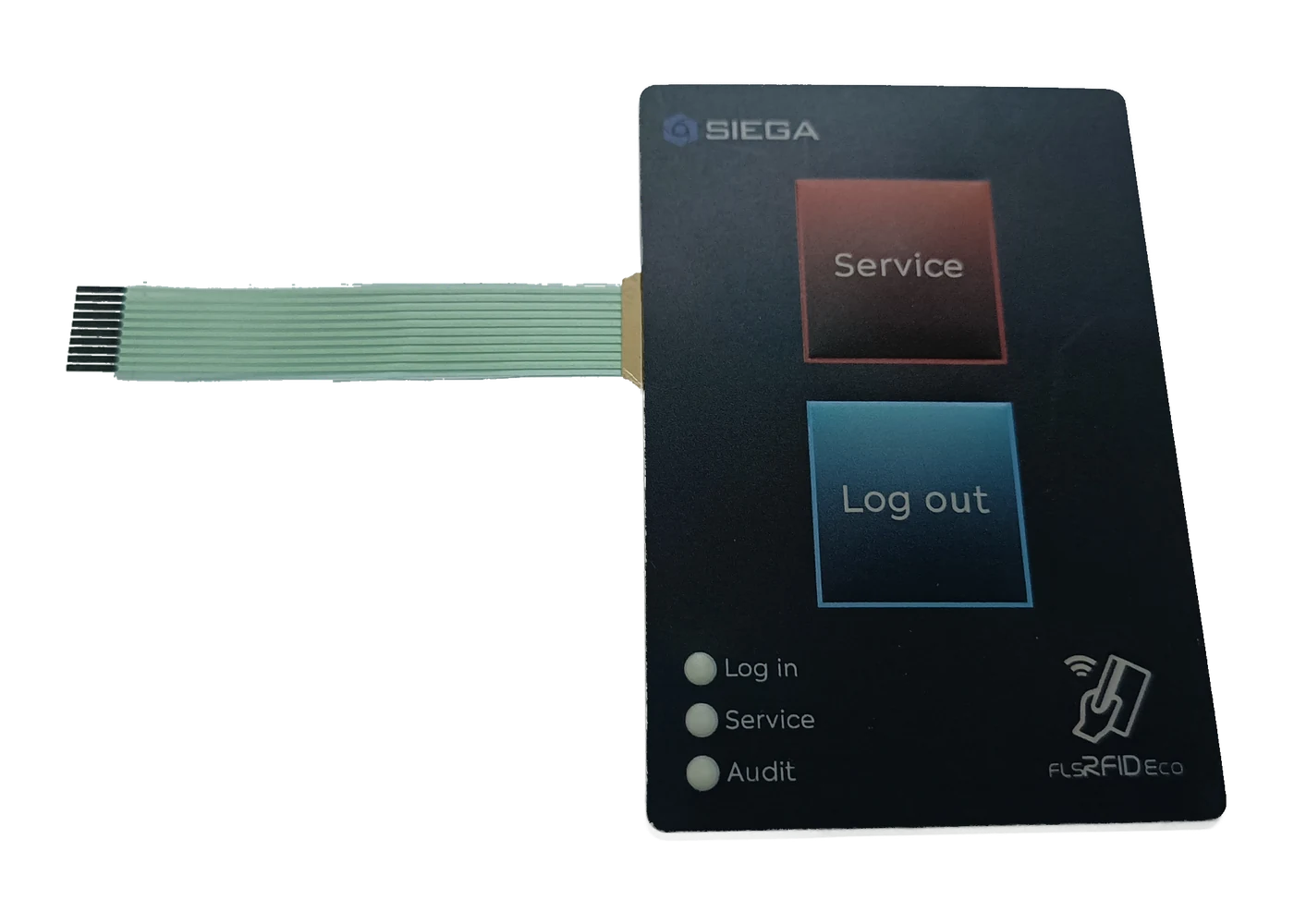
OEM mechanical and electrical engineers who buy custom membrane switches usually discover fit problems after the first ABS or PC+ABS tool is cut. The PET overlay edge collides with a 1.2 mm rib. An LED window sits 0.4 mm off a 3 mm indicator. The 8-pin ZIF tail pinches at a 0.8 mm exit slot. None of those failures is “just a print error.” They are stack-up failures: independent process limits on Autotype-class polyester, DuPont or equivalent silver ink circuits, 3M-class acrylic PSAs, and injection-molded housings that were never added into one loop under ASME Y14.5.
This buyer guide walks that loop feature by feature. It is written for engineers and sourcing teams who need a defensible membrane switch datum design before tooling money is spent. JASPER builds custom membrane switch assemblies for industrial, medical-component, and equipment OEMs.
1. Why Membrane Switch Enclosure Fit Decisions Fail Late
Membrane switch enclosure fit fails late because the switch is often the last custom item released on the bill of materials. SolidWorks or Creo enclosure CAD freezes first. LED positions freeze with the FR4 board. The switch package is treated as a flat sticker that can “absorb” whatever is left. That assumption works until the first production overlay is die-cut from heat-stabilized PET (often 0.15–0.20 mm Autotype or equivalent class) and the pocket was modeled to nominal DXF lines with no clearance.
Three cost shapes show up repeatedly:
- Tooling churn. Steel-rule dies, CO₂ laser programs, and silk screens all move when the pocket grows 0.3 mm after first-article inspection (FAI). Each move burns 1–3 weeks of schedule on a typical industrial HMI program.
- False electrical faults. Keys that land half-off a 12 mm stainless metal dome or silver shorting pad raise contact resistance or create intermittent opens. Field teams chase firmware while the root cause is membrane switch registration tolerance.
- Seal land erosion. Teams chasing a tight cosmetic gap steal width from the 3M 467MP-class adhesive perimeter that was supposed to support an IEC 60529 IP65 or IP67 claim. Water then enters at the cut edge, not through the circuit.
Tolerance stack-up is ordinary mechanical design language under ASME Y14.5 and the ISO GPS system, including ISO 1101:2017. The same math applies here, but the features are thin-film and multi-process: screen print, rim or pillow emboss, laser or steel-rule cut, PSA lamination, and plastic mold shrink of 0.4–0.7% on typical ABS tools. A membrane switch registration tolerance of ±0.25 mm on print-to-cut is useless if the enclosure pocket is ±0.4 mm from the molder and both datums are undefined.
The rest of this article gives a 10-point evaluation framework, a buyer process from RFQ to sample acceptance, and a short list of disqualifiers. Numerical bands are illustrative industry-typical values drawn from published manufacturer design guides, including Higoal International's tolerance guide, JN White's membrane switch design guide, and Butler Technologies' layer anatomy. They are not production guarantees for any one plant.
2. The 10-Point Evaluation Framework for Membrane Switch Tolerance Stack Up
Use these criteria in order when you review drawings or supplier DFM notes. Each criterion includes a acceptance evidence and a release blocker.

2.1 Datum scheme on both enclosure and switch (membrane switch datum design)
Membrane switch datum design starts with one primary plane and two secondary features that both teams can measure on a vision CMM or optical comparator. Typical primary datum A: the front face of the enclosure pocket or the FR4 / aluminum backer plane if the switch mounts to a rigid plate first. Secondary datums B and C: two non-parallel pocket walls, or two Ø3 mm tooling holes that pass through switch and housing on a 50–100 mm baseline.
Without shared datums, “±0.2 mm overall” is a slogan. Print registration, circuit pads, and cut edges each float relative to different origin points in the supplier’s CAM (often Gerber + DXF with mismatched 0,0). Feature control frames from ASME Y14.5 only work when both files name the same A|B|C frame.
Both enclosure drawing and switch drawing show the same datum reference frame (ASME Y14.5 or ISO 1101 language) and state which features are inspected from which datum.
Only overall length/width tolerances; no datum balloons; supplier quotes “industry standard tolerance” with no feature list.
2.2 Full feature loop — cut edge, keys, windows, contacts, tail, enclosure
A complete membrane switch tolerance stack up names every feature that must line up in assembly:
| Feature | Why it sits in the loop |
|---|---|
| Outer cut edge | Pocket fit, gap cosmetics, seal land width |
| Mounting / LED / display cut-outs | Collision with bosses, windows, bezels |
| Printed legend / deadfront | Visual centering on emboss and windows |
| Emboss / key active areas | Finger target vs dome / shorting pad |
| Circuit contact pads | Electrical continuity under the dome |
| Tail exit and connector | Pinch, bend radius, connector float |
| Enclosure pocket walls / ribs | Interference, buckling, light leaks |
| Seal land / rear adhesive edge | IP path vs clearance trade |
If any feature remains unresolved at sample approval, the loop is open.
One assembly view marks every critical feature with a basic dimension and tolerance or a geometric control from the shared datum.
Pretty overlay artwork with no circuit layer in the same coordinate system.
2.3 Membrane switch registration tolerance (print-to-cut and circuit-to-cut)
Membrane switch registration tolerance is the allowed offset between printed graphics (and/or circuit features) and the final cut outline. Higoal's January 2026 guide publishes ±0.25 mm print-to-cut as its standard figure, while JN White publishes process-specific cutting bands rather than one universal registration promise. Treat tighter ±0.10–0.15 mm bands as process- and panel-specific. Circuit-to-cut offsets matter just as much: a 12 mm stainless dome that is centered under the legend but 0.3 mm off the carbon-over-silver pad can still create an intermittent contact.
Registration burns twice when colors stack. Pantone-matched multi-color legends plus selective matte/gloss texture windows add color-to-color error (often managed toward ΔE targets in print QA) before the cut even happens.
Separate callouts for color-to-color, print-to-cut, and circuit-to-cut, each with a measurement method (Keyence/OGP-class optical CMM, vision system, or pin gauges).
Single “registration ±0.1 mm” claim with no process description—often unachievable on 300–400 mm appliance panels cut by steel-rule dies.
2.4 Enclosure pocket clearance and membrane switch enclosure fit
Membrane switch enclosure fit is mostly pocket geometry. Higoal publishes 0.15–0.25 mm side clearance as its design starting point for installation and material movement. That is vendor guidance, not a universal tolerance: validate the gap against the selected PET, temperature range, pocket process, and cosmetic requirement. A zero-clearance press fit can buckle a 0.7–1.5 mm flexible stack or lift the rear adhesive from the mounting surface.
Also budget:
- Corner radii on pocket vs switch (sharp R0 pocket corners vs R1.5–R3 laser/die cuts).
- Ribs under the active area (a 1.0 mm rib under a 12 mm key can create false actuation or dead zones).
- Window ledges that hide or shadow 0603/0805 LED openings by 0.2–0.5 mm.
Pocket dimensions include max material condition thinking: largest switch vs smallest pocket still clears; smallest switch vs largest pocket still covers a continuous ≥2–3 mm seal land.
Pocket modeled as exact DXF of the artwork outline with no gap and no MMC/LMC discussion under ASME Y14.5.
2.5 Layer stack thickness budget
A tactile membrane switch is often six to nine layers (PET graphic overlay, overlay adhesive, dome retainer or top circuit, spacer, bottom circuit, rear adhesive, optional aluminum/FR4 backer), a construction pattern documented in Butler Technologies' January 2026 layer guide. Spacer films commonly sit near 0.005–0.007 in (about 0.13–0.18 mm), and each film and acrylic PSA adds thickness tolerance. Higoal's published table lists ±10% as its standard total-stack band and ±5% as its high-precision band; confirm both against the proposed BOM and inspection method.
Thickness stack-up hits:
- Flushness to a 1–2 mm bezel step.
- Dome travel and 180–350 g actuation force windows.
- ZIF 0.3 mm flex slot fill on 1.0 mm pitch connectors.
- Wet-out and bond build-up of the selected rear adhesive; 3M's 467MP data sheet positions that family for metals and high-surface-energy plastics, so textured or low-surface-energy substrates require separate adhesive validation.
Layer table with material grade, nominal thickness in mm, tolerance, and UL 94 V-0 / VTM-0 callout where the end product requires it.
“Total thickness approx. 1 mm” with no layer BOM and no micrometer FAI plan.
2.6 Tail exit, bend path, and connector float
The tail is where otherwise clean front panels fail in the field. Epec's membrane-switch guidance and the NFI design guide both use a 0.100 in (2.54 mm) smooth bend as a published starting point for a single-layer silver-ink tail, while warning against bends near the connector or tail exit. That figure does not automatically apply to dual-layer tails, stiffened terminations, or etched copper FPC. Exit slots need clearance for the full stack and adhesive, and connector float must not drive the tail into a sharp ABS edge.
For etched copper/polyimide FPC tails, the IPC-2223 family provides the relevant flexible-board design context. Do not transplant a copper-flex bend rule onto a screen-printed silver PET tail without material- and construction-specific validation.
Tail path shown in 3D or section view; strain relief; specified connector family (ZIF vs crimp) matched to vibration environment (IEC 60068-style tests when required).
Tail drawn as a straight ribbon with no exit clearance and no bend note.
2.7 Seal land versus cosmetic gap (IEC 60529 reality check)
If the product claims an IP rating under IEC 60529, the rear adhesive perimeter is a designed feature, not leftover plastic. Tightening membrane switch enclosure fit for a hairline gap can steal seal land. External vent paths, when present, also interact with the same edges.
Minimum continuous adhesive width called out; tail filler or gasket strategy documented; IP claim tied to a test plan, not a brochure adjective.
“IP67 membrane switch” on the RFQ with a 1 mm border and multiple open vents.
2.8 Process capability matched to the drawing
Steel-rule die cutting, laser cutting, and CNC knife cutting do not share the same process capability. Competitor-published bands often show roughly:
| Parameter | Common published standard band | Common published high-precision band |
|---|---|---|
| Overall L/W | ±0.38 mm | ±0.15 mm |
| Hole Ø / position | ±0.25 mm | ±0.10 mm |
| Edge-to-circuit min | 1.27 mm | 0.76 mm |
| Critical cut-outs | often ±0.15 mm class | project-specific |
The standard and high-precision columns summarize Higoal's published bands. JN White and Reliatrace publish different process-specific figures. Treat all three as supplier capability examples, then confirm the selected process with first-article data for the actual panel size and material.
Calling ±0.05 mm on a 400 mm appliance overlay cut by steel rule is a commercial release blocker, not a quality upgrade.
Supplier states process (laser vs die), panel size limit for each tolerance class, and inspection sampling plan.
One universal tolerance line for every feature on every material.
2.9 Sample acceptance criteria and measurement method
Fit is not approved by “eyeballing the sample on the boss’s desk.” Define:
- Which datums the sample is clamped to.
- Which features are measured (optical vs pin).
- Pass/fail numbers for gap, window offset, key-to-dome offset, tail exit.
- How many samples (prototype vs production first article).
Written sample approval checklist shared before build.
Verbal “looks good” email with no dimensions recorded.
2.10 Change control when enclosure or artwork revises
A color change that shifts a window 0.2 mm can break registration even if the cut die is untouched. Enclosure ECO that moves a rib under a key changes actuation. Treat switch artwork revision and housing revision as one configuration.
Linked revision tables; supplier requires re-FAI on datum-affecting ECOs.
Artwork “Rev C” ships into “Rev A” pockets with no re-measure.
3. Step-by-Step Buyer Process (Drawing to Accepted Sample)
This sequence turns the framework into a job you can run with a mechanical engineer and a buyer on the same thread.
Step 1 — Freeze the enclosure datum scheme first
Before RFQ, mark primary and secondary datums on the enclosure CAD in SolidWorks, Creo, or NX. Export a pocket drawing with wall thickness, R2–R5 corner radii, rib heights under the keypad, window ledges, and tail exit slot width/height. If the PCB is the real mounting plane, name that plane as datum A explicitly. Membrane switch datum design cannot start from Illustrator artwork alone.
Step 2 — Build the feature loop on one assembly sketch
On a single sheet, place: outer cut, windows, keys, dome centers, connector, and enclosure edges. Draw the tolerance loop as a chain, not as isolated boxes. A simple text stack is enough:
Enclosure primary datum / pocket face
pocket wall position (± enclosure mold)
switch outer cut (± cut process)
print registration to cut (± print-to-cut)
key/window graphics
circuit pad / dome center (± circuit-to-cut)
tail exit vs slot (± cut + assembly)
That diagram is your membrane switch tolerance stack up in one view.
Step 3 — Issue the RFQ with a real drawing package
Package at minimum:
- DXF/DWG mechanical outline with datums
- Circuit layer (Gerber or equivalent) aligned to the same origin
- Color-separated overlay artwork (Pantone/CMYK, not RGB screenshots)
- Layer stack table (materials + thicknesses)
- Environmental targets (temperature, chemicals, IP if any)
- Explicit question: “List process capability for each critical feature.”
Point suppliers at your prototyping expectations if you need iterative form-fit samples before production tooling.
Step 4 — Compare DFM replies against the 10 criteria
Score each supplier reply on datum clarity, registration callouts, pocket clearance recommendation, stack table, and sample plan. Ignore pure unit-price rank until fit risk is scored. Manufacturers that only paste a generic catalog tolerance line fail criterion 2.8.
Step 5 — Approve first articles against a written checklist
Use a sample approval matrix such as:
| Check | Method | Illustrative pass example* | Result |
|---|---|---|---|
| Outer cut vs pocket gap (each side) | Feeler / optical | ≥0.15 mm and ≤0.40 mm | |
| Window to LED offset | Optical from datum | ≤0.25 mm | |
| Legend center to dome center | Optical | ≤0.25 mm | |
| Circuit pad under dome | Continuity + X-ray/vision as needed | Pad fully under contact area | |
| Tail exit free of pinch | Visual + pull test plan | No sharp bend at slot | |
| Stack thickness | Micrometer at 3 points | Within agreed band | |
| Seal land continuous | Visual + adhesive squeeze-out rules | No voids on perimeter |
*Examples are illustrative starting points, not universal specs. Replace with project numbers.
Record results in the quality file; testing plans for continuity, actuation, and environmental stress sit beside fit checks, not instead of them.
Step 6 — Lock configuration before multi-cavity tools
Only after FAI pass should steel-rule dies or high-volume print screens freeze. If the plastic housing still has open ECOs, keep the switch on soft tooling.
Step 7 — Re-verify on first production lot
Process drift shows up when operators change die pressure or ink viscosity. Spot-check the same datum features on the first production lot, not only on the golden sample.
4. Release Blockers That Disqualify a Drawing Package or Supplier Reply
These override a low quote.
- No shared datums between enclosure and switch files.
- RGB mockups as the only “artwork” with no Pantone/print-ready separations.
- Zero-clearance pocket modeled to the artwork outline.
- Universal ±0.05 mm on large PET panels without process proof.
- IP claim without seal land width or test method.
- Tail exit missing from the 3D model.
- Refusal to state measurement method for registration.
- Artwork and housing revisions unlinked in the ECO process.
- Sample approval by photo only with no dimensions.
- Circuit layer origin different from overlay origin with no transform documented.
Any three of the above is enough to stop a purchase order until DFM is redone.
5. Engineering References and How to Use Them
These sources define drawing language, enclosure protection, flex-circuit context, adhesive behavior, or published supplier capability. A vendor tolerance is evidence of that vendor's stated process band, not proof that every factory or every panel size can hold it.
| Reference | Use in a tolerance review |
|---|---|
| ASME Y14.5-2018 | Datum reference frames, dimensions, and geometric controls on engineering drawings |
| ISO 1101:2017 | ISO GPS symbol language and interpretation of geometrical specifications |
| IEC 60529 consolidated edition | Classification language for enclosure ingress protection; it does not certify the membrane switch by itself |
| IPC board design standards | Flexible-board design context for etched copper/polyimide FPC constructions |
| 3M 467MP technical data sheet | Published adhesive properties, intended substrates, application conditions, and test limitations |
| JN White membrane switch design guide | Public cutting, circuitry, spacing, and tooling examples for supplier comparison |
| Reliatrace membrane switch design guide | Steel-rule, critical-feature, hole-position, hard-tool, and laser examples |
| Higoal tolerance guide | Published print-to-cut, pocket-clearance, overall-size, hole-position, and stack-thickness bands |
| Butler Technologies layer guide | Six-to-nine-layer construction and the function of each layer |
| Epec tail bend guidance | Tail bend location and a published starting radius for a single-layer construction |
| NFI membrane switch design guide | Tail routing, bend, connector, and manufacturing design notes |
6. Frequently Asked Questions
What is a membrane switch tolerance stack up?
It is the combined effect of cut size, print and circuit registration, layer thicknesses, and enclosure features on final alignment of keys, windows, contacts, and the tail. Engineers add those contributors in one loop so assembly still works at worst-case or statistical limits.
What is a typical membrane switch registration tolerance?
Public manufacturer guides often cite about ±0.25 mm for print-to-cut registration on screen-printed overlays, with tighter bands on high-precision laser workflows. Treat those figures as industry-typical starting points and confirm on your panel size and process.
How should membrane switch datum design start?
Start on the enclosure or PCB mounting plane, not on the graphic. Define one primary plane and two secondary features both parties can measure, then reference cut edges, windows, and circuit pads to that frame using ASME Y14.5 or ISO GPS practices.
How much clearance does membrane switch enclosure fit usually need?
Illustrative published tips often recommend roughly 0.15–0.25 mm per side between switch outline and pocket wall for installation and material movement. Large temperature swings, textured paint, and thick stacks may need more; cosmetic appliance panels sometimes accept looser gaps.
When is a tight stack-up the wrong choice?
When the panel is large, purely cosmetic, cost-driven, and the enclosure is still changing weekly. Paying for ±0.10 mm holes on a ±0.5 mm molded bezel wastes money. Tighten only features that affect contact, sealing, or critical windows.
Which standards apply to the drawing language?
ASME Y14.5 and the ISO GPS system (including ISO 1101) cover datum frames and geometric controls. IEC 60529 covers IP coding if sealing is claimed. Flex circuit practice often references the IPC-2223 family for layout context. None of these replace a project-specific FAI plan.
What files should an RFQ include?
Mechanical DXF/DWG with datums, aligned circuit data, color-separated graphics, layer stack table, environmental targets, and a list of critical-to-fit features. Optional: 3D of the pocket and tail path.
How do adhesives change the stack?
Rear and interlayer PSAs add thickness and can squeeze out or fail to wet LSE plastics. Public industrial families such as 3M 467MP-class for smooth metals and 300LSE-class for low-surface-energy plastics are commonly specified; wrong adhesive choice shows up as edge lift that looks like a cut-size error.
What should sample acceptance include?
Measured gaps, window offsets, key-to-dome offsets, stack thickness, tail exit condition, and seal land continuity—each with method and pass/fail numbers agreed before build. Photos alone are not acceptance.
7. What to Do Next
Pick the shared datum, close the feature loop, and put numbers only on features that earn them. Then send the enclosure drawing and the proposed datum scheme to a membrane switch manufacturer that will answer with a layer table, process capability notes, and a sample checklist—not a one-line “standard tolerance” email.
JASPER manufactures custom membrane switch assemblies and can review pocket CAD against circuit and overlay layers as part of normal DFM. Use the 10 criteria above to review the proposed construction before tooling. Start from the custom membrane switches product requirements, use prototyping for form-fit iterations, and keep fit evidence with other testing records.
Export the enclosure pocket drawing with datums and the current switch outline, mark critical windows/keys/tail exit, and request a written stack-up review before any hard tooling is cut.
Check the datum chain before tooling
Send the enclosure drawing, switch artwork, circuit origin, tail route, and acceptance priorities. JASPER will identify open stack-up decisions before sample release.